A kind of ultraviolet LED epitaxy structure and preparation method thereof
An epitaxial structure, ultraviolet technology, applied in the direction of semiconductor devices, electrical components, circuits, etc., can solve the problems of increasing cost, reducing reliability, immature violet LED epitaxial growth technology, etc., reducing the process and improving the overall reliability. , the effect of simplifying subsequent packaging steps
- Summary
- Abstract
- Description
- Claims
- Application Information
AI Technical Summary
Problems solved by technology
Method used
Image

Examples
Embodiment 1
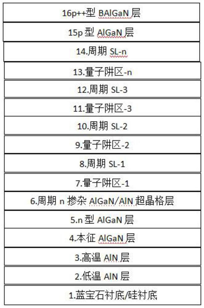
[0086] see figure 1, this embodiment provides an ultraviolet LED epitaxial structure, including a substrate, and a low-temperature AlN layer, a high-temperature AlN layer, an intrinsic AlGaN layer, an n-type AlGaN layer doped with silane, and a doped n-doped AlGaN / AlN superlattice layer of heterosilane, quantum well region-1, superlattice SL region-1, quantum well region-2, superlattice SL region-2, quantum well region-3, supercrystalline Lattice SL region-3, quantum well region-n, superlattice SL region-n, p-type AlGaN layer and magnesium-doped p++ type BAlGaN layer.
[0087] In this embodiment, the thickness of the low-temperature AlN layer is 10 nm; the thickness of the high-temperature AlN layer is 200 nm;
[0088] The thickness of the typical AlGaN layer is 100nm; the thickness of the n-type AlGaN layer doped with silane is 200nm; the doping amount of silane is 10 20 ±1 cm 3 ;
[0089] The n-doped AlGaN / AlN superlattice layer doped with silane is composed of AlGaN an...
Embodiment 2
[0100] This embodiment provides an ultraviolet LED epitaxial structure, including a substrate, and a low-temperature AlN layer, a high-temperature AlN layer, an intrinsic AlGaN layer, an n-type AlGaN layer doped with silane, and a doped Silane n-doped AlGaN / AlN superlattice layer, quantum well region-1, superlattice SL region-1, quantum well region-2, superlattice SL region-2, quantum well region-3, superlattice SL region-3, quantum well region-n, superlattice SL region-n, p-type AlGaN layer and magnesium-doped p++ type BAlGaN layer.
[0101] In this embodiment, the thickness of the low-temperature AlN layer is 10 nm; the thickness of the high-temperature AlN layer is 200 nm;
[0102] The thickness of the typical AlGaN layer is 100nm; the thickness of the n-type AlGaN layer doped with silane is 100nm; the doping amount of silane is 10 20 ±1 cm 3 ;
[0103] The n-doped AlGaN / AlN superlattice layer doped with silane is composed of AlGaN and AlN alternately grown for 10 cycle...
Embodiment 3
[0114] This embodiment provides an ultraviolet LED epitaxial structure, including a substrate, and a low-temperature AlN layer, a high-temperature AlN layer, an intrinsic AlGaN layer, an n-type AlGaN layer doped with silane, and a doped Silane n-doped AlGaN / AlN superlattice layer, quantum well region-1, superlattice SL region-1, quantum well region-2, superlattice SL region-2, quantum well region-3, superlattice SL region-3, quantum well region-n, superlattice SL region-n, p-type AlGaN layer and magnesium-doped p++ type BAlGaN layer.
[0115] In this embodiment, the thickness of the low-temperature AlN layer is 10 nm; the thickness of the high-temperature AlN layer is 200 nm;
[0116] The thickness of the typical AlGaN layer is 100nm; the thickness of the n-type AlGaN layer doped with silane is 300nm; the doping amount of silane is 10 20 ±1 cm 3 ;
[0117] The n-doped AlGaN / AlN superlattice layer doped with silane is composed of AlGaN and AlN alternately grown for 10 cycle...
PUM
| Property | Measurement | Unit |
|---|---|---|
| thickness | aaaaa | aaaaa |
| thickness | aaaaa | aaaaa |
| thickness | aaaaa | aaaaa |
Abstract
Description
Claims
Application Information
 - Generate Ideas
- Intellectual Property
- Life Sciences
- Materials
- Tech Scout
- Unparalleled Data Quality
- Higher Quality Content
- 60% Fewer Hallucinations
Browse by: Latest US Patents, China's latest patents, Technical Efficacy Thesaurus, Application Domain, Technology Topic, Popular Technical Reports.
© 2025 PatSnap. All rights reserved.Legal|Privacy policy|Modern Slavery Act Transparency Statement|Sitemap|About US| Contact US: help@patsnap.com