Novel electric, thermal and mechanical property collaborative environment for electronic product packaging

A technology of electronic products and mechanical characteristics, applied in the direction of electrical digital data processing, special data processing applications, instruments, etc., can solve problems such as signal waveform distortion, interference, and delay generation

Pending Publication Date: 2021-07-16
海安集成电路技术创新中心 +2
View PDF0 Cites 0 Cited by
  • Summary
  • Abstract
  • Description
  • Claims
  • Application Information

AI Technical Summary

Problems solved by technology

When the operating frequency of the system is high, the wire interconnecting the devices should no longer be regarded as a simple wire transparent to the signal, but a parasitic element with time delay and instantaneous impedance distribution, which will cause delay and cause signal waveform distortion , interference, etc.

Method used


Image

  • Novel electric, thermal and mechanical property collaborative environment for electronic product packaging

Examples


Embodiment Construction

[0010] In the following, an integrated design environment of electricity, heat and mechanics applied to packaging design of electronic products according to the present invention will be described in detail with specific examples in conjunction with the accompanying drawings.

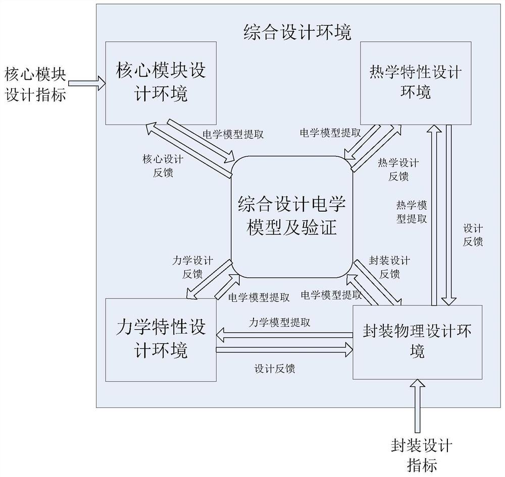
[0011] This embodiment provides an integrated design environment of electricity, heat and mechanics applied to packaging design of electronic products, figure 1 It is a schematic diagram of the realization of the present invention, including the core module design environment, the physical design environment of packaging, the thermal design environment of packaging, the electrical design environment of packaging, and the electrical simulation and verification environment of comprehensive design.

[0012] The core module design environment, according to the performance requirements of the product, carries out the design, simulation and verification of the core circuit of the electronic product and the des...


PUM


Abstract

The invention discloses a novel collaborative environment considering electrical, thermal and mechanical properties of electronic product packaging. Compared with a traditional electronic product design and packaging method and process, the design complexity is greatly reduced, the product design period is shortened, and the one-time design success rate is increased. The method is characterized in that comprehensive, accurate and reconfigurable design parameters and performance and function prediction for electrical, thermal and mechanical characteristics of electronic product packaging are provided on a lumped design platform. By synergistically considering the effects of packaging, thermal and mechanical characteristics on the product performance, in the design stage of the product, the product performance can be optimized from product core design optimization, packaging optimization, thermal optimization and mechanical design optimization according to the aspects of design cost, implementation complexity and the like. Therefore, on one hand, the low-cost realization of the product performance is ensured, on the other hand, a plurality of design freedom degrees are provided, the complexity of realizing the performance is reduced, and most importantly, the expectation of the product performance can be accurately evaluated in the product design stage, and the design iteration is reduced.

Description

technical field [0001] The invention relates to the fields of packaging design for electronic circuits, automation of electronic circuit design, and computer aided design of electronic circuits. Background technique [0002] With the continuous advancement of electronic technology and integrated circuit technology, the clock rate of digital systems is getting higher and higher, and the signal edge rate is getting faster and faster. From the perspective of electrical performance, the interconnection between high-speed signals is no longer smooth and transparent. The impact of PCB wire interconnection and board layer characteristics on the system can no longer be simply ignored. There are gold wires, metal wires on the substrate, vias and corners, stubs, solder balls, etc. in the package interconnection. In low-frequency signals, they are often regarded as simple transmission lines. When the operating frequency of the system is high, the wire interconnecting the devices shoul...

Claims


Application Information

Patent Timeline
IPC IPC(8): G06F30/398G06F119/14G06F119/08
Inventor 蒋乐乐陆宇马松沈立
Owner 海安集成电路技术创新中心
Why Eureka
Try Eureka