Array substrate and manufacturing method thereof

An array substrate and substrate technology, which is applied in semiconductor/solid-state device manufacturing, electrical components, electrical solid-state devices, etc., can solve the problems of short-circuiting of the light-shielding layer, exposure of the light-shielding layer, short-circuit, etc., so as to avoid the second metal layer and the above-mentioned The effect of short-circuiting the shading layer and improving the quality

Active Publication Date: 2021-07-09
SHENZHEN CHINA STAR OPTOELECTRONICS SEMICON DISPLAY TECH CO LTD
View PDF9 Cites 0 Cited by
  • Summary
  • Abstract
  • Description
  • Claims
  • Application Information

AI Technical Summary

Problems solved by technology

[0004]However, during the manufacturing process of the array substrate, the oxide layer and the first metal layer are likely to be spaced apart from each other due to machine offset or unstable etching process. The buffer layer in the gap will be etched in the subsequent process, so that the light-shielding layer is exposed, so that the second metal layer will short the first metal layer, the oxide layer, and the light-shielding layer together, resulting in the risk of short circuit

Method used


Image

  • Array substrate and manufacturing method thereof
  • Array substrate and manufacturing method thereof
  • Array substrate and manufacturing method thereof

Examples


Embodiment Construction

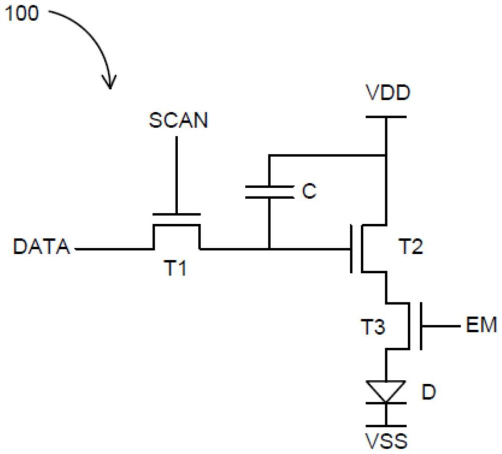
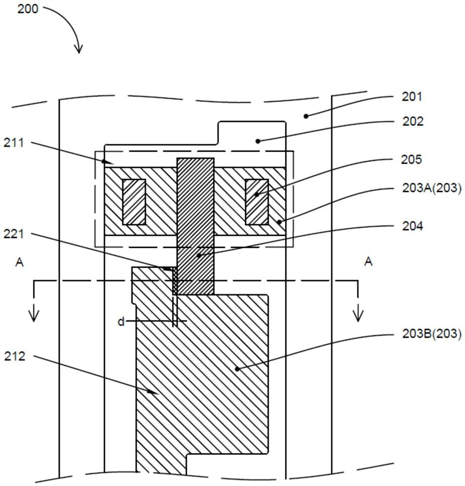
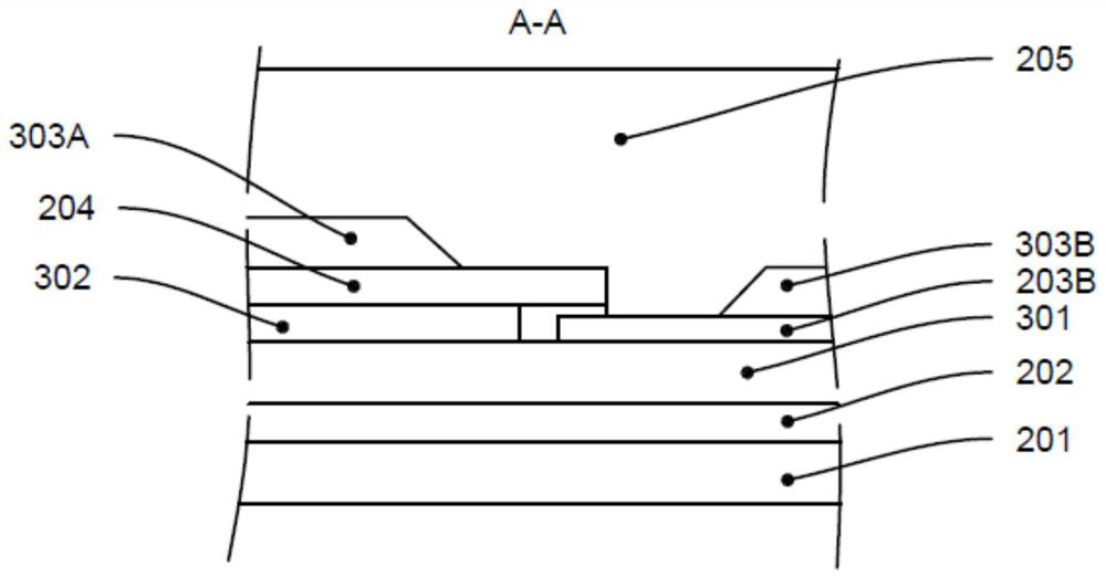
[0056] The following will clearly and completely describe the technical solutions in the embodiments of the present invention with reference to the accompanying drawings in the embodiments of the present invention. Obviously, the described embodiments are only some, not all, embodiments of the present invention. Based on the embodiments of the present invention, all other embodiments obtained by those skilled in the art without creative efforts fall within the protection scope of the present invention. In addition, it should be understood that the specific embodiments described here are only used to illustrate and explain the present invention, and are not intended to limit the present invention. In the present invention, unless stated to the contrary, the used orientation words such as "up" and "down" usually refer to up and down in the actual use or working state of the device, specifically the direction of the drawing in the drawings ; while "inside" and "outside" refer to ...


PUM

PropertyMeasurementUnit
thicknessaaaaaaaaaa
thicknessaaaaaaaaaa
thicknessaaaaaaaaaa

Abstract

The invention discloses an array substrate and a manufacturing method thereof. The array substrate comprises a substrate, a shading layer, a buffer layer, an oxide layer, a gate insulation layer, a first metal layer, a pixel driving circuit and a second metal layer. The pixel driving circuit comprises a first transistor and a storage capacitor, and at the bridge joint of the first transistor and the storage capacitor, the projections of the first metal layer and the oxide layer on the substrate are at least partially overlapped. Therefore, electrical performance abnormity caused by short circuit of the second metal layer and the light shielding layer can be effectively avoided.

Description

technical field [0001] The present invention relates to the field of display technology, in particular to an array substrate and a manufacturing method thereof. Background technique [0002] Thin Film Transistor (Thin Film Transistor, TFT) array (Array) substrate is currently the main component in LCD (Liquid Crystal Display: liquid crystal display) and AMOLED (Active-matrix organic light emitting diode: active-matrix organic electroluminescent diode) devices. Components. The array substrate usually includes a plurality of gate scanning lines and a plurality of data lines, the plurality of gate scanning lines and the plurality of data lines are perpendicular to each other and form a plurality of pixel units, and each pixel unit is provided with a TFT, a pixel electrode and a storage capacitors, etc. A pixel unit generally includes a first metal layer and a second metal layer, wherein a gate is formed in the first metal layer, and a source and a drain are formed in the seco...

Claims


Application Information

Patent Timeline
Patent Type & Authority Applications(China)
IPC IPC(8): H01L27/12H01L21/84
CPCH01L27/1255H01L27/1244H01L27/1222H01L27/127H01L27/1259
Inventor 张鹏刘方梅
Owner SHENZHEN CHINA STAR OPTOELECTRONICS SEMICON DISPLAY TECH CO LTD
Why Eureka
Try Eureka