Base terminal bonding pad structure, lens driving device, camera device and electronic product
The technology of a lens driving device and a camera device is applied in the direction of electromechanical devices, motor generator connectors, circuits, etc., and can solve problems such as difficult solder entering between conductive components and pads, weak soldering, and virtual soldering, etc., to achieve Solve soldering process problems, facilitate dispensing and fixing, and increase the effect of contact area
- Summary
- Abstract
- Description
- Claims
- Application Information
AI Technical Summary
Problems solved by technology
Method used
Image
Examples
Embodiment 1
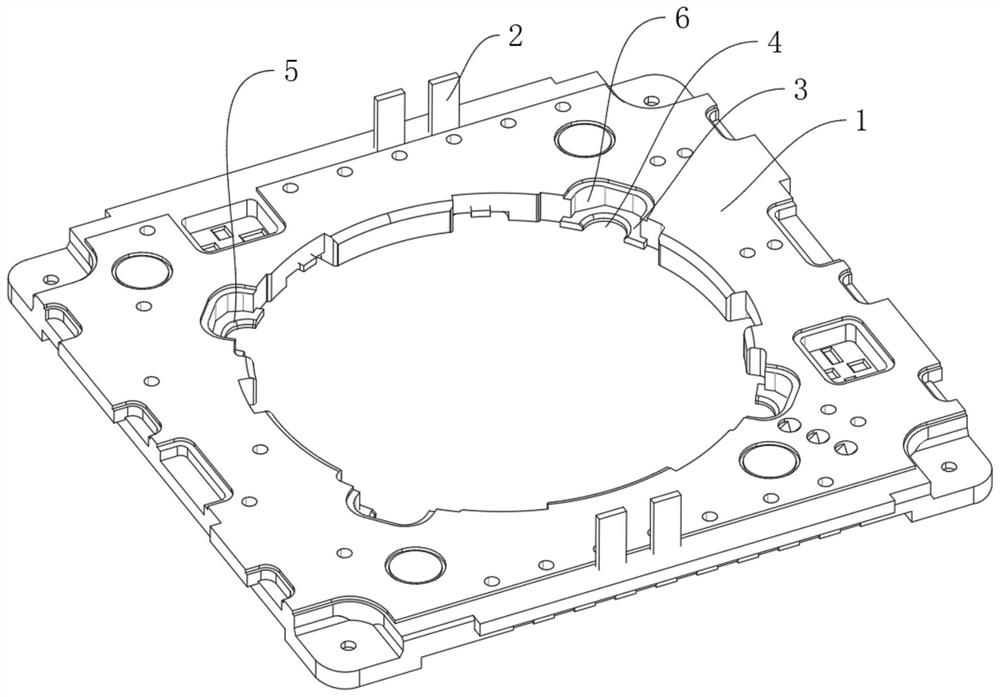
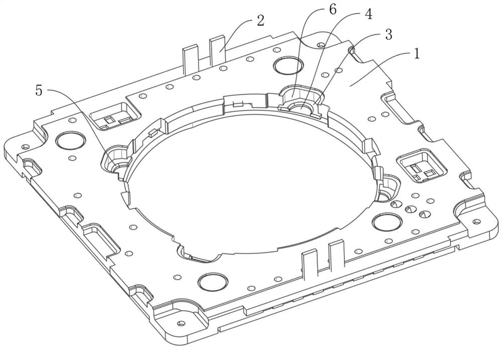
[0034] Embodiment 1: as Figure 1 to Figure 4 As shown, there is a notch on the side wall of the pad 3 facing the center of the base body 1, the notch is a C-shaped notch 4, and a chamfer 5 is provided on the edge of the C-shaped notch 4, and the conductive element corresponding to the pad 3 The device is attached to the pad 3 and covers the C-shaped notch 4. In this embodiment, the conductive component can be an FPC board, and the FPC board is fixed on the surface of the base body 1 facing the direction of the lens. In this embodiment, the chamfer 5 is located at the edge of the C-shaped notch 4 on the side away from the conductive components.
[0035] When soldering the pad 3 and the conductive component (that is, the FPC board), the solder paste is set at the position corresponding to the C-shaped notch 4 of the conductive component, and the solder paste is attached to the position of the chamfer 5 and the pad 3 is away from the surface of the conductive component. , throu...
Embodiment 2
[0038] Embodiment 2, differs from Embodiment 1 in that: as Figure 5 As shown, the chamfer 5 is set at the edge of the side of the pad 3 that is attached to the conductive component, that is, the chamfer 5 is located between the pad 3 and the conductive component. When soldering, the solder paste melts into the position of the chamfer 5, and The chamfer 5 forms a cavity for containing solder paste between the pad 3 and the conductive components, and effectively increases the contact area between the pad 3 and the solder paste, thereby improving the strength between the pad 3 and the conductive components.
Embodiment 3
[0039] Embodiment 3, differs from implementation 1, embodiment 2 in that: as Figure 6 As shown, the two edges of the C-shaped notch 4 are provided with chamfers 5. At this time, the size of the chamfers 5 is smaller than the size of the chamfers 5 in Embodiment 1 and Embodiment 2, but the upper and lower sides of the C-shaped notch 4 are provided with chamfers. 5 Effectively increase the solder paste holding space, increase the contact area, and improve the welding strength.
PUM
 Abstract
Description
Claims
Application Information
 - R&D Engineer
- R&D Manager
- IP Professional
- Industry Leading Data Capabilities
- Powerful AI technology
- Patent DNA Extraction
Browse by: Latest US Patents, China's latest patents, Technical Efficacy Thesaurus, Application Domain, Technology Topic, Popular Technical Reports.
© 2024 PatSnap. All rights reserved.Legal|Privacy policy|Modern Slavery Act Transparency Statement|Sitemap|About US| Contact US: help@patsnap.com


