Tungsten oxide-based memristor embedded with Ti or Al nano island array and preparation method of tungsten oxide-based memristor
A technology of tungsten oxide and memristor, which is applied in the direction of electrical components, etc., can solve the problems of high working voltage, large variation range of device performance parameters, and restrictions on the application of memristor devices
- Summary
- Abstract
- Description
- Claims
- Application Information
AI Technical Summary
Problems solved by technology
Method used
Image
Examples
Embodiment 1
[0046] (1) Put a two-inch silicon wafer into acetone, isopropanol and absolute ethanol in turn for 5 min, respectively, take it out, wash it with water three times, and use an air gun (N 2 ) to dry, and put it on the drying table to dry the water.
[0047] (2) Put the cleaned silicon wafer into the furnace of the plasma-enhanced chemical vapor deposition instrument, heat it at 300°C for 5′30″, and grow 300nm silicon oxide on the surface of the silicon wafer to obtain SiO 2 / Si.
[0048] (3) SiO 2 / Si is placed in the chamber of the magnetron sputtering instrument, with metal Ti as the target material, the sputtering power is 150W, the sputtering time is 1230s, the sputtering gas environment is Ar, and a 100nm Ti layer is deposited by DC sputtering to obtain Ti / SiO 2 / Si. Using metal Pt as the target material, the sputtering power is 60W, the sputtering time is 740s, the sputtering gas environment is Ar, and a 100nm Pt layer is deposited by DC sputtering to obtain Pt / Ti / ...
Embodiment 2
[0056] Embodiment 2 (comparative example)
[0057] Other steps are with embodiment 1, the Pt / Ti / SiO that makes in the present embodiment 2 / Si without the transfer of ultra-thin AAO, a 5nm thick Ti layer was directly deposited to produce WO with a photolithographic pattern x / Ti / Pt / Ti / SiO 2 / Si devices.
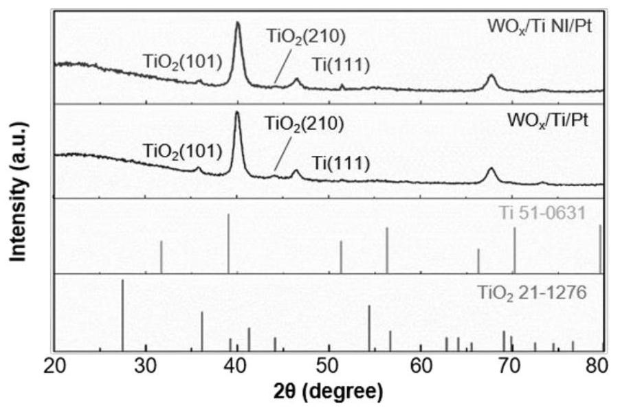
[0058] Through XRD analysis, it was found that the Ti embedded in the device was partially oxidized to form TiO x ( image 3 ). According to the XPS analysis, with the voltage sweep cycle, the WO in the device (2.57) containing Ti nano-islands x The ratio of oxygen vacancies to lattice oxygen in the layer is higher than ( Figure 7 A, B). The I-V cycle curve is tested by a semiconductor parameter analyzer, and the accumulated probability statistics of the data obtained from the test are obtained to determine the WO x When the Pt electrode of the / Ti / Pt device is scanned with a voltage of -2V, the forming process of the device occurs at -1.6V ( Figure 5 C), V SET an...
Embodiment 3
[0060] The other steps are the same as in Example 1. In this example, the Ti target in step (6) is replaced by an Al target, still using The rate of deposition is 250s. Finally, a WO with a photolithographic pattern is obtained x / Al NI / Pt / Ti / SiO 2 / Si devices.
[0061] Test its I-V cycle curve by a semiconductor parameter analyzer. Through the electrical performance test, WO x The / Al NI / Pt device does not require the Forming process and has a negative differential resistance phenomenon ( Figure 8 A). V SET and V RESET The average values are -0.59V and 0.51V, and the coefficients of variation are 3.36% and 1.86%, V SET and V RESET The coefficient of variation and WO x / Ti NI / Pt devices are similar, with a small scatter ( Figure 8 B).
PUM
| Property | Measurement | Unit |
|---|---|---|
| The average diameter | aaaaa | aaaaa |
Abstract
Description
Claims
Application Information
 - R&D
- Intellectual Property
- Life Sciences
- Materials
- Tech Scout
- Unparalleled Data Quality
- Higher Quality Content
- 60% Fewer Hallucinations
Browse by: Latest US Patents, China's latest patents, Technical Efficacy Thesaurus, Application Domain, Technology Topic, Popular Technical Reports.
© 2025 PatSnap. All rights reserved.Legal|Privacy policy|Modern Slavery Act Transparency Statement|Sitemap|About US| Contact US: help@patsnap.com


