Inert atmosphere cooling device for baking battery material and application method thereof
A battery material, inert atmosphere technology, applied in electrical components, generators/motors, processing discharged materials, etc., can solve problems affecting the normal process and cycle of battery material preparation, inability to obtain fine crystallinity, and easy electrode materials. Oxidation by air, etc., to achieve the effect of improving final performance, high subcooling, compact and reasonable structure
- Summary
- Abstract
- Description
- Claims
- Application Information
AI Technical Summary
Problems solved by technology
Method used
Image
Examples
Embodiment 1
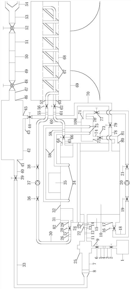
[0053] see figure 1 , which shows a battery material roasting cooling system under an inert atmosphere, the roasting cooling system includes a battery material roasting device and a battery material inert atmosphere cooling device.
[0054] The battery material roasting device includes a tube furnace 69 for roasting the battery material 108, which has an internal roasting area 68 inside. Specifically, the tube furnace 69 is an open tube furnace with dual temperature zones.
[0055] The battery material inert atmosphere cooling device is mainly composed of three parts: a radiation-convection comprehensive cooling and heat recovery device, a semiconductor module thermoelectric power generation device, and an argon preheating and recycling device.
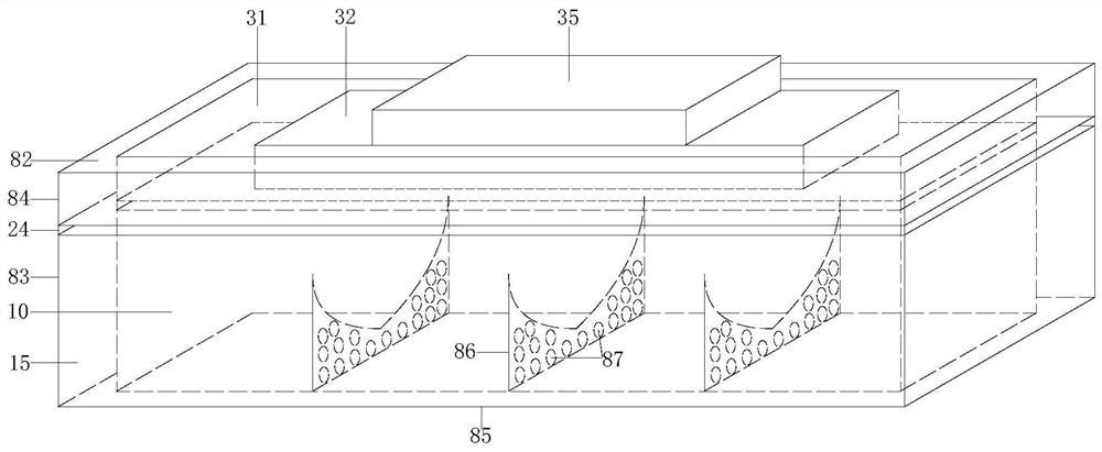
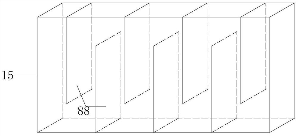
[0056] Radiation-convection comprehensive cooling and heat recovery device is mainly composed of vortex tube cold end 11, cooling chamber 10, water cooling cooling interlayer 15, small cooling water pump 20, heat transfer oil chamber ...
Embodiment 2
[0100] This embodiment is basically the same as Embodiment 1, the main difference is: as Figure 8As shown, in the present embodiment, the semiconductor thermoelectric power generation module 35 includes: two n-type semiconductors 91 and two p-type semiconductors 92, and the n-type semiconductors 91 and p-type semiconductors 92 are arranged alternately (that is, corresponding to the first one from left to right in the figure). One and the third are p-type semiconductors 92, the second and the fourth are n-type semiconductors 91), and adjacent n-type semiconductors 91 and p-type semiconductors 92 are arranged at intervals; two semiconductor hot end metal plates 90 and three A semiconductor cold-end metal plate 102, a semiconductor hot-end metal plate 90 and a semiconductor cold-end metal plate 102 are respectively located on both sides of the n-type semiconductor 91 and the p-type semiconductor 92, and the adjacent n-type semiconductor 91 and the p-type semiconductor 92 form a s...
PUM
 Abstract
Description
Claims
Application Information
 - R&D
- Intellectual Property
- Life Sciences
- Materials
- Tech Scout
- Unparalleled Data Quality
- Higher Quality Content
- 60% Fewer Hallucinations
Browse by: Latest US Patents, China's latest patents, Technical Efficacy Thesaurus, Application Domain, Technology Topic, Popular Technical Reports.
© 2025 PatSnap. All rights reserved.Legal|Privacy policy|Modern Slavery Act Transparency Statement|Sitemap|About US| Contact US: help@patsnap.com


