


Quick Research
Generate reliable direction feasibility study reports for your R&D in just a few steps.

Technical Q&A
Discover and master advanced knowledge NOW. Basics, ideas, possibilities, all at once.

Find Solutions
As an expert in R&D theories, this can generate solutions to your technical problems instantly.

Evaluate Feasibility
Analyze your overall solution with one click, know your potential R&D risks in advance.

Monitor Landscape
Get weekly tech updates, stay abreast of the latest tech innovations and key insights.
High-yield wafer-level filter chip packaging structure and method
A chip packaging structure and filter technology, which is applied in the manufacturing of electric solid state devices, semiconductor devices, and semiconductor/solid state devices, etc., can solve the problems of large product size, inconsistent product matching, and high cost.
- Summary
- Abstract
- Description
- Claims
- Application Information
AI Technical Summary
Problems solved by technology
Method used
Image

Examples
Embodiment 1
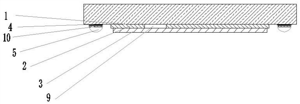
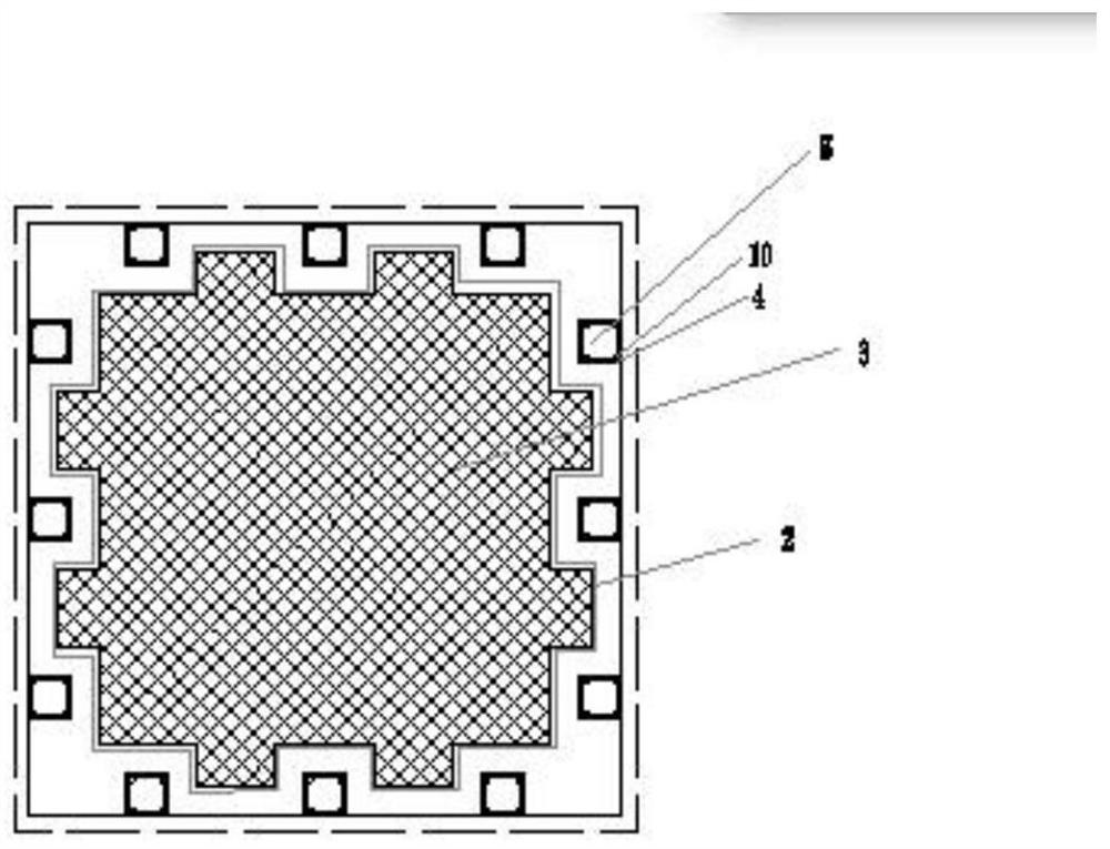
[0029] Such as Figure 1 to Figure 4 As shown, a high-yield wafer level 1 filter chip packaging structure, filter chip and substrate 6, the filter chip is connected to the substrate 6, the filter chip includes a wafer 1, a plurality of welding pads 4. The cofferdam 2 and the cover 3, the welding pad 4 is arranged beside the wafer 1 with a plurality of welding pads 4, the wafer 1 is surrounded by a cofferdam 2, and above the cofferdam 2 is a A cover 3, the cover 3 is closely attached to the top of the cofferdam 2, a sealed cavity 9 is formed between the wafer 1, the cofferdam 2 and the cover 3, and a welding layer 10 is electroplated or chemically plated on the welding pad 4, and the Solder balls or gold balls 5 are arranged above the solder layer 10;
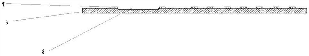
[0030] The substrate 6 is provided with a plurality of metal pads 7 and solder resist oil, the metal pads 7 are soldered to the solder balls or gold balls 5, and grooves 8 are arranged between the plurality of metal pads 7 , t...
Embodiment 2
[0038] Such as Figure 5 Shown, a kind of high yield filter chip packaging method, described method comprises:
[0039] Step 1: Fabricate the cofferdam 2 on the wafer 1 by using glue exposure and development technology, the cofferdam 2 surrounds the wafer 1; the cofferdam 2 is arranged between the wafer 1 and the solder Between the pads 4, the glue coating speed formed by the cofferdam 2 is between 500-1000rpm, the exposure energy of the cofferdam 2 is 150-250mj, the development time of the cofferdam 2 is 200-280s, and the cofferdam 2 is formed During the process, the main rotation speed of glue coating is preferably 800RPM, the exposure energy is 200mj, and the developing time is 240s. The width of the cofferdam 2 is greater than 10um, which is convenient for the operation of step 2.
[0040] Step 2: On the cofferdam 2, the cover 3 is made by film exposure and development, and a sealed cavity 9 is formed between the chip, the cofferdam 2 and the cover 3; the cover 3 is prefe...
PUM
| Property | Measurement | Unit |
|---|---|---|
| Thickness | aaaaa | aaaaa |
| Thickness | aaaaa | aaaaa |
| Thickness | aaaaa | aaaaa |
Abstract
Description
Claims
Application Information
 - R&D Engineer
- R&D Manager
- IP Professional
- Industry Leading Data Capabilities
- Powerful AI technology
- Patent DNA Extraction
Browse by: Latest US Patents, China's latest patents, Technical Efficacy Thesaurus, Application Domain, Technology Topic, Popular Technical Reports.
© 2024 PatSnap. All rights reserved.Legal|Privacy policy|Modern Slavery Act Transparency Statement|Sitemap|About US| Contact US: help@patsnap.com