
Sp3-bonded carbon materials, methods of manufacturing and uses thereof

A composite material and bonding technology, applied in chemical instruments and methods, metal material coating technology, nano-carbon, etc., can solve problems such as inappropriate

Pending Publication Date: 2021-05-07
马德雷与马埃斯特拉天主教教皇大学
View PDF11 Cites 2 Cited by
  • Summary
  • Abstract
  • Description
  • Claims
  • Application Information

AI Technical Summary

Problems solved by technology

In particular, there are no known methods for producing such materials that are suitable for scaling up and adapting to the requirements of various industries such as the electronics industry
Furthermore, many putative routes for such materials considered in the literature suggest the use of high temperatures and / or high pressures, and are therefore not suitable for example to produce such materials on temperature-sensitive and / or pressure-sensitive materials and equipment

Method used


Image

  • Sp3-bonded carbon materials, methods of manufacturing and uses thereof
  • Sp3-bonded carbon materials, methods of manufacturing and uses thereof
  • Sp3-bonded carbon materials, methods of manufacturing and uses thereof

Examples


Embodiment 1

[0080] Commercial chemical vapor deposition (CVD) graphene films deposited on 3 mm ultrafine copper transmission electron microscopy (TEM) grids (2000 mesh) as received were used as graphene material (from Graphene Supermarket, SKU# SKU-TEM-CU-2000-025). by CVD by CH 4 Graphene was grown on Ni substrates at 1000°C and transferred to a commercial TEM grid using a polymer-free transfer method as described in W. Regan et al. (2010) to minimize contamination. The thickness of the CVD graphene film is 0.3nm to 2nm (1 to 6 monolayers). Typical graphene coverage of a TEM grid is 60% to 90%.

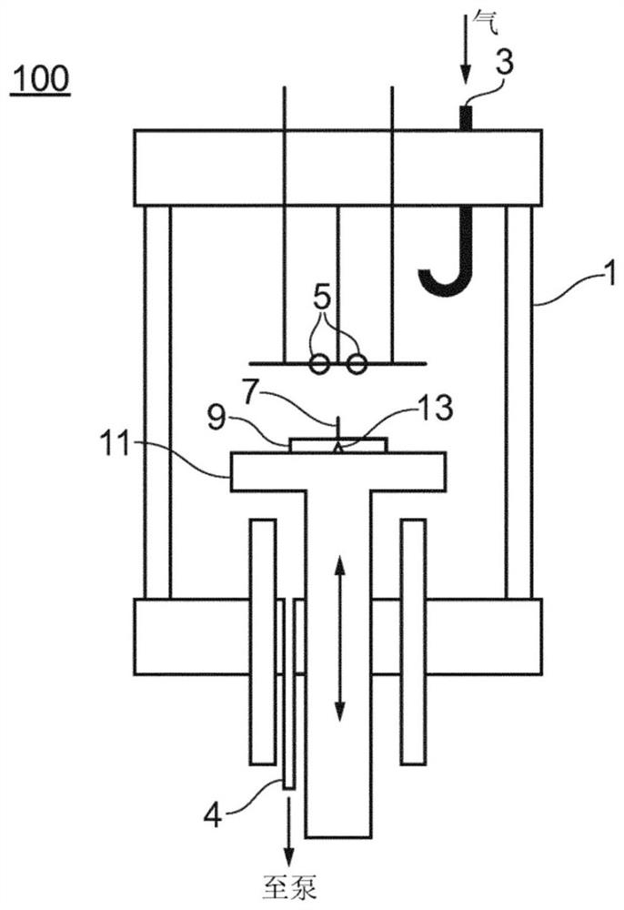
[0081] Hydrogenation and subsequent few-layer graphene to ultrathin crystalline sp 3 Structural transformation of bonded carbon sheets. The schematic diagram of the system is in figure 1 shown in and described above.

[0082] The reactor is a six-way cross stainless steel vacuum chamber. It was fluid cooled (15% water, 75% ethylene glycol at 18° C.) with brazed copper tubes covered with a...


PUM

PropertyMeasurementUnit
thicknessaaaaaaaaaa
cover factoraaaaaaaaaa

Abstract

The present invention provides an ultrathin and crystalline sp3-bonded carbon sheet, a stack structure, heterostructure and composite material comprising said ultrathin and crystalline sp3-bonded carbon sheet, and a method of manufacture of ultrathin and crystalline sp3-bonded carbon sheets. The method comprises the steps of providing a few-layer graphene starting material, disposing the few-layer graphene starting material on a substrate within a chemical vapour deposition chamber comprising a vacuum chamber and a feed gas inlet, and flowing a feed gas comprising hydrogen over the substrate at a substrate temperature of 325 DEG C or less and a pressure of 100 Torr or less to at least partially convert the few-layer graphene starting material into ultrathin and crystalline sp3-bonded carbon sheets. The method according to the present invention is the first method for successful production of ultrathin and crystalline sp3-bonded carbon sheets, including e.g. lonsdaleite sheets and diamond sheets. Advantageously it may also be relatively low cost, low waste, may avoid the use of complex apparatus having multiple components, and may allow operation under mild processing conditions.

Description

technical field [0001] The present invention relates to sp-based 3 Materials of bonded carbon, methods of manufacture and uses thereof, and particularly, though not exclusively, to ultra-thin (few-layer) crystalline sp 3 Bonded carbon materials, methods of manufacture and uses thereof. Background technique [0002] Theoretical work suggests that materials such as few-layer diamond and carbon materials consisting of few-atom-layer (FL) hexagonal carbon (lonsdaleite) (alternatively named "diamane" as proposed by Chernozatonskii et al. (2009)) have great technological potential. prospect. In diamane, sp 3 The bonded carbon atoms are arranged in a hexagonal lattice. Few-atom-layer hexagonal carbon can be considered as the sp of few-layer graphene 3 Hybrid counterparts. In this paper, bilayer diamane (bilayer diamane) similar to bilayer graphene (bilayer graphene (2LG), trilayer graphene (3LG) and few-layer graphene (FLG) , 2LD), three-layer diamane (trilayer diamane, 3LD)...

Claims


Application Information

Patent Timeline
Patent Type & Authority Applications(China)
IPC IPC(8): C01B32/194C01B32/25
CPCC01B32/194C01B32/25C01B32/05C01B32/26C01B2204/04C01P2002/20C01P2002/82C23C16/26
Inventor 法布里斯·皮亚扎
Owner 马德雷与马埃斯特拉天主教教皇大学
Learn More