Optical waveguide element, preparation method thereof and holographic optical waveguide display equipment
A technology of optical waveguide and components, which is applied in the field of optics, can solve the problems of complex structure of holographic waveguide lens, small selectivity of grating diffraction angle, complex post-processing, etc., to achieve improved size shrinkage and diffraction efficiency, excellent optical waveguide imaging effect, The effect of simple production process
- Summary
- Abstract
- Description
- Claims
- Application Information
AI Technical Summary
Problems solved by technology
Method used
Image

Examples
preparation example Construction
[0190] A second aspect of the present invention provides a method for preparing the optical waveguide element of the first aspect, comprising the following steps:
[0191] The step of preparing photopolymer film 102;
[0192] The step of composite molding the carrier 101 and the photopolymer film 102;
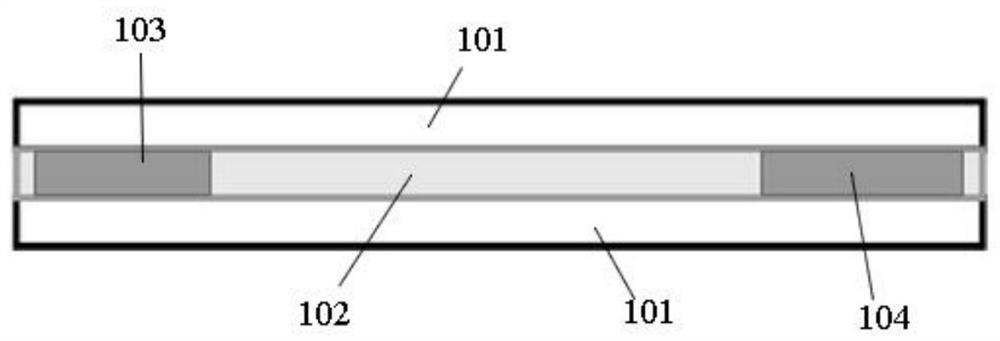
[0193] The step of forming a grating structure, the photopolymer film 102 has at least one light-coupling region 103 and at least one light-coupling region 104, the light-coupling region 103 is not connected to the light-coupling region 104,
[0194] A grating structure is formed in the light coupling region 103 and the light coupling region 104 respectively.
[0195] The present invention is not particularly limited to the step of composite molding the carrier 101 and the photopolymer film 102 first and the step of forming the grating structure first, and may be the step of composite molding the carrier 101 and the photopolymer film 102 first, and then Forming the grating st...
Embodiment 1
[0228] An optical waveguide element is prepared according to the following steps:
[0229] 1) In a dark room or red light environment, mix 10mL of the polymer (obtained by heating at 100°C) and 2mg of silica microsphere spacers with an average particle size of 20μm to form a mixture, and raise the temperature Stir at 100°C for 4 hours until uniformly mixed;
[0230] 2) Maintain 100°C, apply the mixed solution obtained in step (1) on a 1mm thick glass substrate with a size of 20mm×70mm under red light, and then cover the upper surface of the mixed solution with another piece with a size of 20mm A 1mm thick glass substrate of ×70mm is cooled to room temperature to obtain a solid photopolymer dry plate;
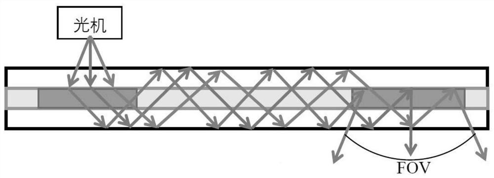
[0231] 3) Interferentially expose one side of the dry plate obtained in step (2) after 532nm laser beam expansion and beam splitting (see attached Figure 5 ), the exposure area is 15mm×15mm, forming a volume holographic grating structure; the dry plate is exposed in the mode ...
Embodiment 2
[0239] The same method as in Example 1, but the exposure energy density is at 8mJ / cm 2 , and the resulting photopolymer dry film component content is shown in Table 2 below:
[0240] Table 2
[0241] composition content Basic Red 2 0.2% N-phenylglycine 0.8% 2-(4-Chlorophenyl)-4,5-diphenylimidazole 1% 2-naphthylthioethyl acrylate (n=1.620) 33% 9,9-bis(methylacrylate) fluorene (n=1.606) 11% Cellulose acetate butyrate (n=1.475) 22% N-vinylpyrrolidone 32%
[0242] The diffraction efficiency of the optical waveguide element obtained in this embodiment is greater than 95%, the angle selectivity reaches ±12°, the exposure is sensitive, and the refractive index modulation degree reaches 0.08.
PUM
| Property | Measurement | Unit |
|---|---|---|
| thickness | aaaaa | aaaaa |
| thickness | aaaaa | aaaaa |
| wavelength | aaaaa | aaaaa |
Abstract
Description
Claims
Application Information
 - R&D
- Intellectual Property
- Life Sciences
- Materials
- Tech Scout
- Unparalleled Data Quality
- Higher Quality Content
- 60% Fewer Hallucinations
Browse by: Latest US Patents, China's latest patents, Technical Efficacy Thesaurus, Application Domain, Technology Topic, Popular Technical Reports.
© 2025 PatSnap. All rights reserved.Legal|Privacy policy|Modern Slavery Act Transparency Statement|Sitemap|About US| Contact US: help@patsnap.com