Light emitting diode epitaxial wafer and preparation method thereof

A technology of light-emitting diodes and epitaxial wafers, which is applied in the direction of electrical components, circuits, semiconductor devices, etc., and can solve the problems affecting the uniformity of light-emitting diode epitaxial wafers, the surface of light-emitting diode epitaxial wafers is not smooth enough, and the height difference of light-emitting diode epitaxial wafers is large And other problems, to achieve the effect of increasing thickness, uniform thickness, and improving uniformity of light emission

Active Publication Date: 2021-04-20
HC SEMITEK SUZHOU
View PDF13 Cites 2 Cited by
  • Summary
  • Abstract
  • Description
  • Claims
  • Application Information

AI Technical Summary

Problems solved by technology

The first n-type GaN layer, multi-quantum well layer, and p-type GaN layer require higher growth temperatures, and at high temperatures, the center region of the substrate is more likely to accumulate heat than the edge region of the substrate, resulting in the center of the substrate The temperature of the region is higher than the temperature of the edge region of the substrate, and the temperature of the center region of the substrate is too high, which will lead to the decomposition of the epitaxial structure grown in the center region of the substrate, and the decomposition of the epitaxial structure grown in the center region of the substrate is relatively poor. The decomposition of the epitaxial structure grown in the edge region of the bottom is serious, resulting in a large height difference between the edge of the surface of the finally obtained LED epitaxial wafer and the center of the surface, and the surface of the LED epitaxial wafer is not smooth enough, which affects the quality of the LED epitaxial wafer. Luminous Uniformity

Method used


Image

  • Light emitting diode epitaxial wafer and preparation method thereof
  • Light emitting diode epitaxial wafer and preparation method thereof
  • Light emitting diode epitaxial wafer and preparation method thereof

Examples


Embodiment Construction

[0032] In order to make the purpose, technical solution and advantages of the present invention clearer, the embodiments of the present disclosure will be further described in detail below in conjunction with the accompanying drawings.

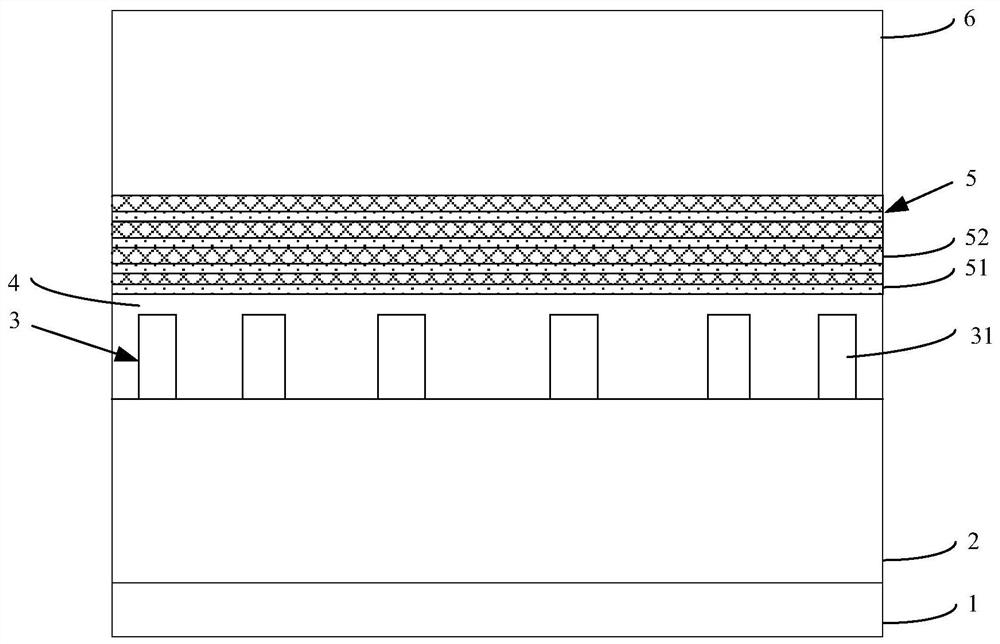
[0033] figure 1 It is a schematic structural diagram of a light-emitting diode epitaxial wafer provided by an embodiment of the present disclosure. Refer to figure 1 It can be seen that the embodiment of the present disclosure provides a light-emitting diode epitaxial wafer, and the light-emitting diode epitaxial wafer includes a substrate and a first n-type GaN layer 2, SiO 2 An adjustment layer 3 , a second n-type GaN layer 4 , a multi-quantum well layer 5 and a p-type GaN layer 6 .

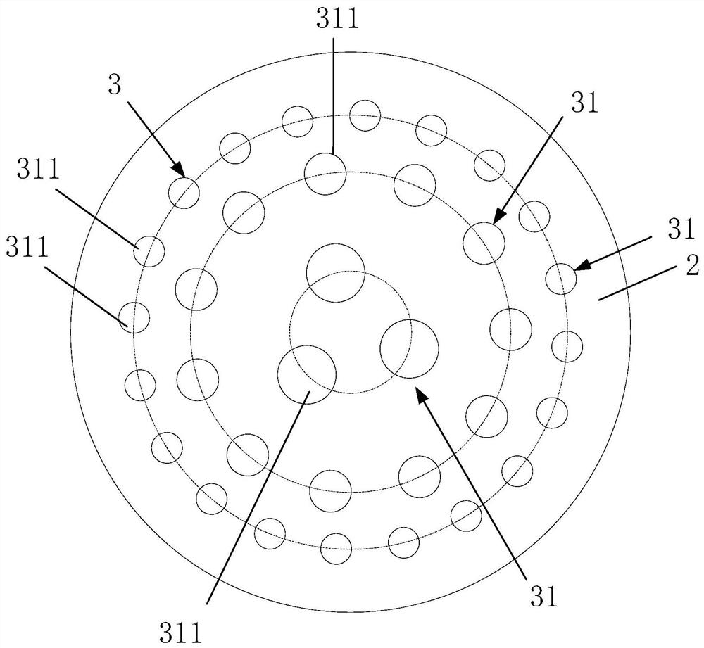
[0034] SiO 2 The adjustment layer 3 includes a plurality of concentric SiO2 distributed at intervals on the surface of the first n-type GaN layer 2 2 Adjustment ring 31, multiple concentric SiO 2 The center of the adjustment ring 31 is the center of the sur...


PUM

PropertyMeasurementUnit
Diameteraaaaaaaaaa
Heightaaaaaaaaaa

Abstract

The invention discloses a light emitting diode epitaxial wafer and a preparation method thereof, and belongs to the field of light emitting diode manufacturing. A SiO2 adjusting layer is added on a first n-type GaN layer, the SiO2 adjusting layer comprises a plurality of concentric SiO2 adjusting circular rings distributed on the surface of the first n-type GaN layer at intervals, the circle centers of the concentric SiO2 adjusting circular rings are the circle center of the surface of the first n-type GaN layer, and each SiO2 adjusting circular ring comprises a plurality of SiO2 adjusting columns distributed at equal intervals. The diameter of the SiO2 adjusting columns is reduced along with the increase of the diameter of the SiO2 adjusting circular rings, and the growth speed of a second n-type GaN layer near the circle center of a substrate is slightly faster than the growth speed of the second n-type GaN layer near the edge of the substrate, so that the thickness difference formed between the area near the edge and the area near the circle center due to temperature is counteracted, the overall growth thickness of the second n-type GaN layer is more uniform, and the light emitting uniformity of the light emitting diode is improved.

Description

technical field [0001] The invention relates to the field of light-emitting diode production, in particular to a light-emitting diode epitaxial wafer and a preparation method thereof. Background technique [0002] LED (English: Light Emitting Diode, Chinese: Light Emitting Diode), a light emitting diode is a semiconductor electronic component that can emit light. As an efficient, environmentally friendly and green new solid-state lighting source, it is being rapidly and widely used, such as traffic lights, car interior and exterior lights, urban landscape lighting, mobile phone backlight, etc. Improving the luminous efficiency of chips is the goal that LEDs are constantly pursuing. [0003] During the preparation of light-emitting diode epitaxial wafers, the substrate needs to be placed in the groove of the tray, the edge and bottom of the tray surface are heated and heated, and the reactive gas and reactive metal source are deposited on the upper surface of the substrate. ...

Claims


Application Information

Patent Timeline
IPC IPC(8): H01L33/20H01L33/02H01L33/00
Inventor 王群郭炳磊葛永晖董彬忠李鹏
Owner HC SEMITEK SUZHOU
Why Eureka
Try Eureka