A stacked three-dimensional package component structure and fabrication method

A component structure and three-dimensional packaging technology, applied in the direction of electrical components, semiconductor devices, electric solid devices, etc., can solve the problems of poor microwave repeatability, not easy to repair, low reliability, etc., to solve the problem of heat dissipation and matching, Good microwave transmission performance and the effect of improving package integration

Active Publication Date: 2022-07-22
NO 55 INST CHINA ELECTRONIC SCI & TECHNOLOGYGROUP CO LTD
View PDF3 Cites 0 Cited by
  • Summary
  • Abstract
  • Description
  • Claims
  • Application Information

AI Technical Summary

Problems solved by technology

The internal substrates of the components are usually interconnected by bonding, which is difficult to meet the requirements of three-dimensional stacking; the components are generally connected by coaxial connectors, ball grid array welding, metal elastic body or button connectors, etc.
Ordinary soldering interconnection requires a large distance between connectors, and it is not easy to repair; while the reliability of ball grid array welding between components is low, and it is not easy to repair; metal elastic body or button connectors can be tightly connected At the same time, there is no need for welding, so it is easy to repair, but the microwave repeatability of the connection between the metal elastic body and the fur button is not good, and microwave reflection is easy to occur, so it is not suitable for millimeter wave high frequency transmission

Method used


Image

  • A stacked three-dimensional package component structure and fabrication method
  • A stacked three-dimensional package component structure and fabrication method
  • A stacked three-dimensional package component structure and fabrication method

Examples


Embodiment Construction

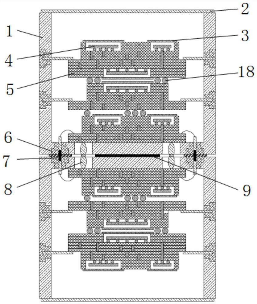
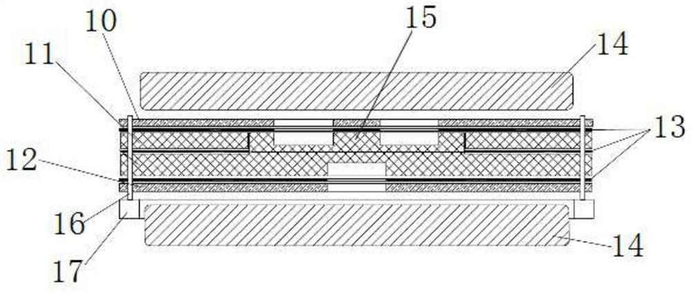
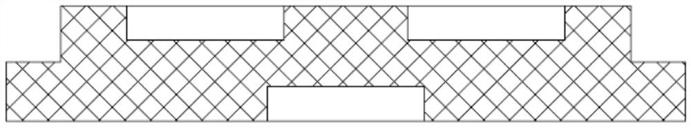
[0062] The present invention will now be described in further detail with reference to the accompanying drawings. These drawings are all simplified schematic diagrams, and only illustrate the basic structure of the present invention in a schematic manner, so they only show the structures related to the present invention.

[0063] In order to overcome the problems in the background technology, the present invention provides a stacked three-dimensional package assembly structure, which is suitable for the preparation of a multilayer ceramic substrate 5 with multiple upper and lower cavities, the vertical interconnection of multiple substrates inside the assembly, and between sub-assemblies. Detachable combination form.

[0064] Generally, it includes several sub-assemblies, each sub-assembly is provided with a transmission port, and adjacent sub-assemblies are interconnected at the transmission port through a consolidation device to realize stacking; The ceramic substrates are ...


PUM

PropertyMeasurementUnit
thicknessaaaaaaaaaa
thicknessaaaaaaaaaa
depthaaaaaaaaaa

Abstract

The invention relates to a stacked three-dimensional package assembly structure and a manufacturing method. The assembly structure includes a plurality of subassemblies, each subassembly is provided with a transmission port, and adjacent subassemblies are interconnected at the transmission port through a consolidation device to achieve stacking; each subassembly Including a casing, a plurality of multilayer ceramic substrates are arranged in the casing, BGA packaging is used for stacking and interconnection between the plurality of multilayer ceramic substrates, a cavity is opened on the surface or bottom of each multilayer ceramic substrate, and BGA soldering is installed in each cavity. The chip is welded inside the multi-layer ceramic substrate through BGA packaging; the cavity opened in the multi-layer ceramic substrate can be partially sealed; the opening of the entire casing is covered with a cover plate for sealing; the invention solves the problem of existing in the background technology. Therefore, a stacked three-dimensional package assembly structure is provided, which not only has high integration, excellent microwave performance, and good reliability, but also facilitates assembly disassembly.

Description

technical field [0001] The invention relates to a stacked three-dimensional package component structure and a manufacturing method, and belongs to the field of three-dimensional package of radio frequency components. Background technique [0002] The most commonly used packaging form of RF microsystem components is the structure of low temperature co-fired ceramic (LTCC) and aluminum matrix composite metal shell. The LTCC substrate has low dielectric loss and high hardness, can meet complex wiring requirements, and has the conditions to achieve multi-channel transmission. It is the most commonly used RF microsystem component packaging form at home and abroad. The aluminum-based composite metal shell provides signal input and output channels, heat dissipation channels, mechanical support and a protected working environment for the LTCC substrate. [0003] As the performance indicators of components become more and more stringent, RF microsystem components must develop toward...

Claims


Application Information

Patent Timeline
Patent Type & Authority Patents(China)
IPC IPC(8): H01L25/07H01L25/00H01L23/498H01L23/60
CPCH01L25/071H01L25/50H01L23/49816H01L23/49838H01L23/60
Inventor 庞学满谢新根陈骏陈雨钊
Owner NO 55 INST CHINA ELECTRONIC SCI & TECHNOLOGYGROUP CO LTD
Why Eureka
Try Eureka