Rigid-flex circuit board and manufacturing method thereof

A combination of soft and hard, manufacturing method technology, applied in the direction of printed circuit manufacturing, printed circuit, printed circuit, etc., can solve problems such as open circuit, uneven thickness, etc.

Inactive Publication Date: 2021-03-19
QING DING PRECISION ELECTRONICS HUAIAN CO LTD +1
View PDF9 Cites 0 Cited by
  • Summary
  • Abstract
  • Description
  • Claims
  • Application Information

AI Technical Summary

Problems solved by technology

Therefore, the area where the protective layer 202 is buried in the hard board is thicker than the area where the protective layer 202 is not covered. This uneven thickness will cause colloid to remain in the blind hole when the blind hole is formed in the area where the protective layer 202 is embedded, thereby filling the hole. Metal copper cannot be plated on the hole, resulting in open circuit

Method used


Image

  • Rigid-flex circuit board and manufacturing method thereof
  • Rigid-flex circuit board and manufacturing method thereof
  • Rigid-flex circuit board and manufacturing method thereof

Examples


Embodiment Construction

[0046] The following will clearly and completely describe the technical solutions in the embodiments of the present invention with reference to the accompanying drawings in the embodiments of the present invention. Obviously, the described embodiments are only some, not all, embodiments of the present invention. Based on the embodiments of the present invention, all other embodiments obtained by persons of ordinary skill in the art without making creative efforts belong to the protection scope of the present invention.

[0047] Unless otherwise defined, all technical and scientific terms used herein have the same meaning as commonly understood by one of ordinary skill in the technical field of the invention. The terms used herein in the description of the present invention are for the purpose of describing specific embodiments only, and are not intended to limit the present invention.

[0048] Some embodiments of the present invention will be described in detail below in conju...


PUM


Abstract

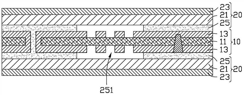
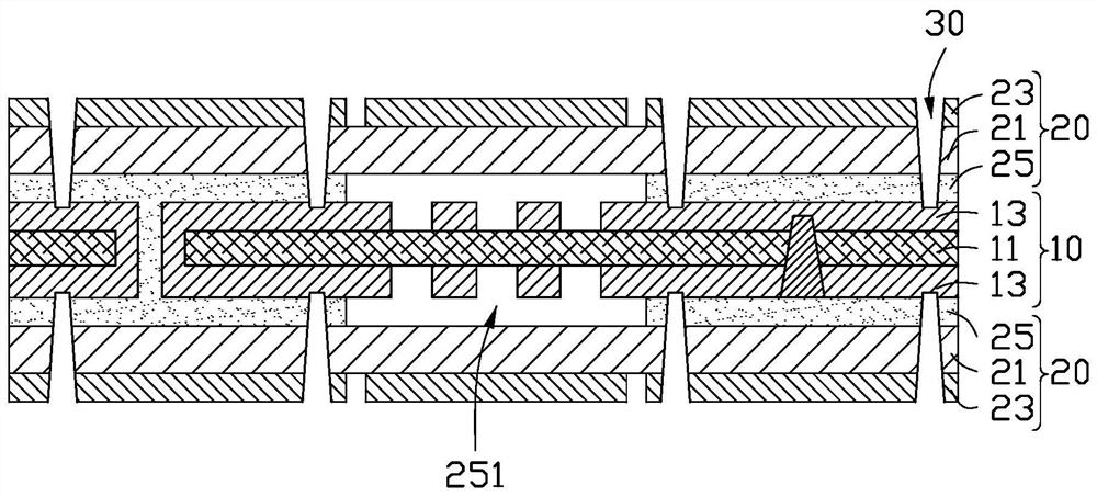
The invention provides a rigid-flex circuit board. The rigid-flex circuit board comprises: an inner-layer substrate, wherein the inner-layer substrate comprises a flexible base layer and a circuit layer formed on the surface of the flexible base layer; a rigid substrate, which covers a part of the surface of the circuit layer, wherein the part, provided with the rigid substrate, of the rigid-flexcircuit board is a layer adding area, the part, not provided with the rigid substrate, of the rigid-flex circuit board is a flexible area, and at least one first conductive block connected with the circuit layer is arranged in the rigid substrate; an outer-layer substrate, which comprises an outer copper layer, a dielectric layer and a bonding layer, wherein the bonding layer covers the surfaces of the circuit layer and the hard substrate, the dielectric layer covers the surface of the bonding layer, and the outer copper layer covers the surface, corresponding to the layer adding area, of thedielectric layer; and a solder mask layer, which covers the surface of the outer copper layer. According to the rigid-flex circuit board, the dielectric layer and the bonding layer are used for replacing a protective layer to cover the flexible area of the inner-layer substrate, so the problem of open circuit caused by uneven thickness of the layer adding area is solved, and the flexibility of theflexible area is improved. The invention further provides a manufacturing method of the rigid-flex circuit board.

Description

technical field [0001] The invention relates to the field of circuit boards and their manufacture, in particular to a soft-rigid circuit board and a manufacturing method thereof. Background technique [0002] With the development of chip technology, the requirements for the quality and size of rigid-flex circuit boards are becoming increasingly stringent. Rigid-flex boards are more and more widely used due to their advantages of easy assembly, good signal transmission reliability, and thinness. [0003] see Figure 10 , in order to control the aspect ratio of the existing rigid-flex board, the protective layer 202 (Coverlay, CVL) of the flexible circuit board 201 is changed to be partially embedded, specifically extending a section from the flexible circuit board 201 to the rigid board 203 . Therefore, the area where the protective layer 202 is buried in the hard board is thicker than the area where the protective layer 202 is not covered. This uneven thickness will cause ...

Claims


Application Information

Patent Timeline
Patent Type & Authority Applications(China)
IPC IPC(8): H05K1/14H05K3/28H05K3/36
CPCH05K1/147H05K3/282H05K3/361H05K2201/0154
Inventor 李卫祥
Owner QING DING PRECISION ELECTRONICS HUAIAN CO LTD
Why Eureka
Try Eureka