
Photoelectric detector and using method thereof

A technology of photodetectors and devices, applied in the field of photodetectors, which can solve the problems of reduced responsivity, saturated absorption at the incident end, and distortion of photoelectric conversion signals

Active Publication Date: 2021-03-19
WUHAN POST & TELECOMM RES INST CO LTD +1
View PDF8 Cites 2 Cited by
  • Summary
  • Abstract
  • Description
  • Claims
  • Application Information

AI Technical Summary

Problems solved by technology

[0004] Aiming at one of the defects existing in the prior art, the purpose of this application is to provide a photodetector and its use method to solve the problem of saturated absorption easily occurring at the incident end of the waveguide-type silicon-germanium photodetector in the related art to cause photoelectric conversion Problems with signal distortion and reduced responsiveness

Method used

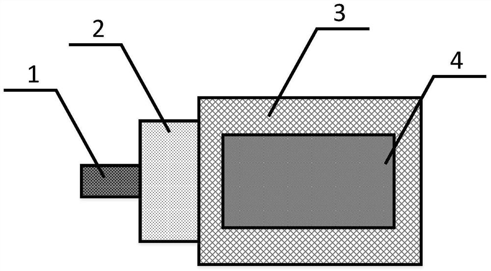
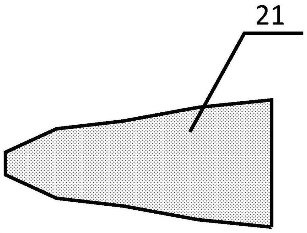
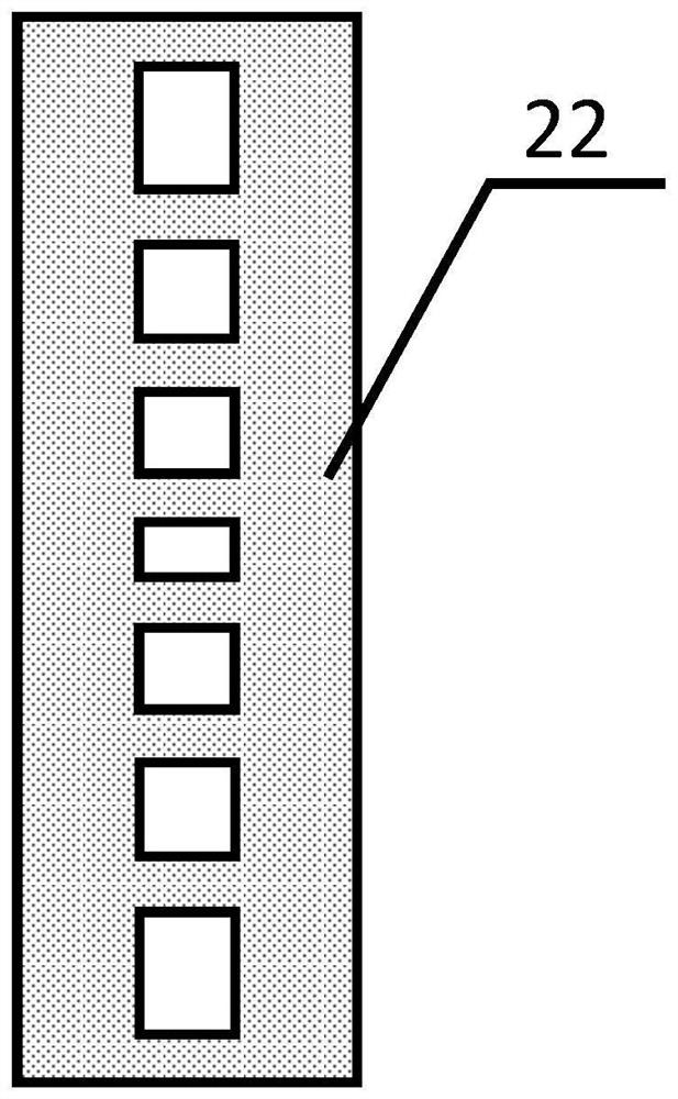

Image

  • Photoelectric detector and using method thereof
  • Photoelectric detector and using method thereof
  • Photoelectric detector and using method thereof

Examples


Embodiment Construction

[0033] In order to make the purpose, technical solution and advantages of the present application clearer, the present invention will be further described in detail below in conjunction with the accompanying drawings and embodiments. It should be understood that the specific embodiments described here are only used to explain the present invention, not to limit the present invention. In addition, the technical features involved in the various embodiments of the present invention described below can be combined with each other as long as they do not constitute a conflict with each other.

[0034] The embodiment of the present application provides a photodetector and its use method, which can solve the problem that the incident end of the waveguide-type silicon-germanium photodetector in the related art is prone to saturated absorption, which causes signal distortion in photoelectric conversion and reduces the responsivity. .

[0035] Such as figure 1 As shown, the photodetect...


PUM


Abstract

The invention discloses a photoelectric detector and a using method thereof, and relates to the field of optical communication integrated devices. The photoelectric detector comprises an incident waveguide used for propagating signal light; a silicon layer, provided with a germanium absorption region, and the germanium absorption region being used for detecting signal light and converting the signal light into an electric signal; a focusing device, used for focusing the signal light of the incident waveguide to the silicon layer under the germanium absorption region, and the width of a light beam converged when the signal light reaches the incident end of the germanium absorption region through the focusing device is larger than that of the germanium absorption region. The using method comprises the steps that signal light enters the focusing device through the incident waveguide; the focusing device focuses the signal light to the silicon layer right below the germanium absorption region, and enables the width of a converged light beam to be greater than the width of the germanium absorption region when the signal light reaches the incident end of the germanium absorption region;and the germanium absorption region converts the signal light into an electric signal. According to the photoelectric detector, the saturated absorption power of the photoelectric detector can be improved, signal distortion does not occur during photoelectric conversion, and the responsivity of the device can also be improved.

Description

technical field [0001] The present application relates to the field of optical communication integrated devices, in particular to a photodetector and a method for using the same. Background technique [0002] At present, silicon-based photonic chips have the advantages of compatibility with standard semiconductor processes, low cost, and high integration, and are gradually being widely adopted by the industry. In the field of optical communication, the device used at the receiving end of the silicon-on-chip integrated system is a waveguide-type silicon-germanium photodetector. [0003] In the related art, the waveguide-type germanium-silicon photodetector adopts a square structure, and light is incident from one end and exits from the corresponding other end, undergoing one-way absorption. However, since the incident light power decreases rapidly from the input end to the output end, in the case of high-power incident, the incident end is prone to saturated absorption, whic...

Claims


Application Information

Patent Timeline
IPC IPC(8): H01L31/09H01L31/0232
CPCH01L31/09H01L31/02327
Inventor 陈代高肖希王磊胡晓张宇光余少华
Owner WUHAN POST & TELECOMM RES INST CO LTD
Learn More