Package structure

A packaging structure and packaging material technology, applied in the direction of electrical components, electrical solid devices, circuits, etc., can solve the problems of large packaging structure size, large power loss, and high overall inductance

Pending Publication Date: 2021-03-19
ANCORA SEMICON INC
View PDF5 Cites 0 Cited by
  • Summary
  • Abstract
  • Description
  • Claims
  • Application Information

AI Technical Summary

Problems solved by technology

Due to the long heat dissipation path of the metal wire, and considering the requirements of the number of wires and the wire distance, the size of the formed package structure is large, and it has the disadvantages of high overall inductance and large power loss.

Method used


Image

  • Package structure
  • Package structure
  • Package structure

Examples


Embodiment Construction

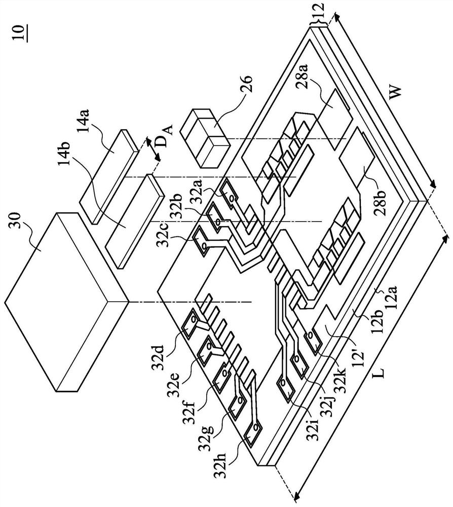
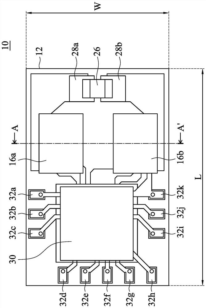
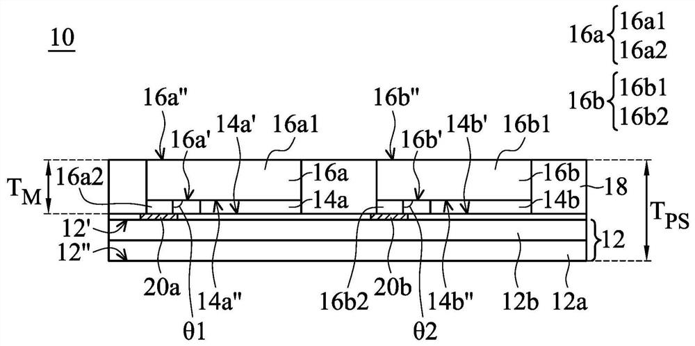
[0059] see figure 1 , figure 2 , image 3 , according to an embodiment of the present invention, a packaging structure 10 is provided. figure 1 is an exploded view of the package structure 10 . figure 2 is a top view of the package structure 10 . image 3 for along figure 2 A cross-sectional view of the package structure 10 obtained by the A-A' section line.

[0060] Such as figure 1 , figure 2 , image 3 As shown, the packaging structure 10 includes a substrate 12 , a first active element 14 a , a second active element 14 b , a first metal portion 16 a , a second metal portion 16 b and an encapsulation material 18 . The substrate 12 has a first surface 12' and a second surface 12", and the second surface 12" is opposite to the first surface 12'. The first active element 14a has a first surface 14a' and a second surface 14a", and the second surface 14a" is opposite to the first surface 14a'. The second active element 14b has a first surface 14b' and a second surfac...


PUM

PropertyMeasurementUnit
diameteraaaaaaaaaa
thicknessaaaaaaaaaa
angleaaaaaaaaaa

Abstract

The invention provides a package structure. The package structure includes a substrate, a plurality of active components, a plurality of separated metal parts and an encapsulation material. The substrate has a first surface and a second surface. Each active component has a first surface and a second surface. Each metal part has a first surface and a second surface. The first surface of each activecomponent is connected to the first surface of the substrate. The first surface of one metal part is connected to the second surface of one active component. Each metal part extends to connect to thefirst surface of the substrate. The encapsulation material covers the first surface of the substrate and surrounds the active components and the metal parts. The second surface of each metal part andthe second surface of the substrate are exposed from the encapsulation material.

Description

technical field [0001] The invention relates to a package structure, in particular to a package structure with double-side heat dissipation. Background technique [0002] A system in package (SIP) is a functional electronic system that includes two or more heterogeneous semiconductor dies (often from different technology nodes optimized for their respective functions), Usually includes, for example, active components, passive components and driver integrated circuits. The physical form of the system-in-package is a module, which depends on the final application. In the package structure, such a module can include logic chips, memory chips, integrated passive devices (integrated passive devices, IPDs), RF filters, sensor detectors, heat sinks, antennas, connectors and / or power chips. [0003] In a traditional system-in-package (SIP), the active components are connected to the electrodes of the substrate through a wire bonding process. Heat conduction toward the substrate i...

Claims


Application Information

Patent Timeline
Patent Type & Authority Applications(China)
IPC IPC(8): H01L23/367H01L23/373H01L23/49
CPCH01L23/3736H01L23/367H01L23/3677H01L23/49H01L25/072H01L25/0655H01L25/16H01L25/18H01L2924/18161H01L23/49838H01L23/49822H01L2924/16152H01L2924/16235H01L2924/16251H01L2224/16237H01L24/16H01L2224/13155H01L2224/131H01L2224/13144H01L2224/13147H01L2924/00014H01L2924/014H01L23/3157H01L23/3675H01L24/08
Inventor 李仁智杨长暻王良丞叶时有
Owner ANCORA SEMICON INC
Why Eureka
Try Eureka