Wafer cutting method

A cutting method and wafer technology, applied in electrical components, semiconductor/solid-state device manufacturing, circuits, etc., can solve problems such as splits, wafer appearance damage, cracks, etc., and achieve the effect of precise control of cutting amount

Active Publication Date: 2021-03-05
HUA HONG SEMICON WUXI LTD
View PDF1 Cites 1 Cited by
  • Summary
  • Abstract
  • Description
  • Claims
  • Application Information

AI Technical Summary

Problems solved by technology

[0005] The current laser ring cutting process adopts a fixed time method for ring cutting process. This fixed time is based on the experience value accumulated in the previous process, and the cutting effect is roughly estimated by the cutting time. This time is difficult to adjust according to the actual situation. , there is a problem of insufficient or too long cutting time. Insufficient cutting time will lead to the connection between the support ring and the effective die area. During the ring removal process, cracks will be caused, and in severe cases, lobes will be generated; too long cutting time will cause, WPH (number of wafers per hour) is too low, and burns the UV film supporting the wafer, causing damage and defects on the appearance of the wafer

Method used


Image

  • Wafer cutting method

Examples


Embodiment Construction

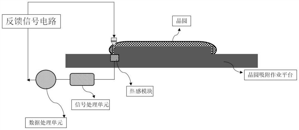
[0019] The wafer cutting method described in the present invention is mainly aimed at ring cutting of the wafer. According to the principle of cutting, due to the severe friction between the cutting head and the wafer in the cutting area, the heat in the cutting area accumulates, and the temperature continues to rise. After the wafer is cut through, the cutting head no longer rubs against the wafer, and the cutting area will appear sudden change in temperature. Such as figure 1 As shown, the entire cutting system includes a cutting head, which realizes circular cutting of the wafer, and also includes a thermal module, a signal processing unit, a data processing unit, and a feedback signal circuit. When the dicing unit ring-cuts the wafer, a thermal module is arranged under the wafer. Specifically, after the wafer is adsorbed on the cutting table, the thermal module is installed directly below the area with a radius of 130-150mm of the wafer. The thermal module and the cuttin...


PUM

PropertyMeasurementUnit
Radiusaaaaaaaaaa
Thicknessaaaaaaaaaa

Abstract

The invention discloses a wafer cutting method, which comprises the following steps that: when a cutting unit carries out ring cutting on a wafer, a thermal inductance module is arranged below the wafer, and the thermal inductance module and a cutting head are respectively arranged on two sides of the wafer; when the thermal induction module conducts cutting, the change of the temperature of a cutting area in the cutting process can be inducted in real time, signals are transmitted to the signal processing unit, the signal processing unit transmits thermal induction signals to the data processing unit, the data processing unit controls the cutting head through the feedback signal loop, and the cutting amount is accurately controlled.

Description

technical field [0001] The invention relates to the field of semiconductor device manufacturing, in particular to a wafer cutting method. Background technique [0002] With the rapid development of IC technology, the requirements for chip integration, speed and reliability are getting higher and higher, which requires chips to be smaller and thinner. At the same time, in order to reduce the production cost of a single chip and better control product performance, more and more chip types have begun to use 12-inch silicon wafers for production. [0003] The typical process of 12-inch wafer backside thinning technology in the field of power devices is TAIKO grinding, backside wet etching, backside metallization, ring cutting and ring removal. When the TAIKO process grinds the wafer, it will keep the peripheral edge of the wafer (about 3mm), and only grind and thin the inside of the circle. The advantage of the TAIKO process is to reduce wafer warpage and improve wafer strengt...

Claims


Application Information

Patent Timeline
IPC IPC(8): H01L21/78H01L21/67H01L21/66
CPCH01L21/78H01L22/26H01L22/12H01L21/67253
Inventor 肖酉苏亚青谭秀文
Owner HUA HONG SEMICON WUXI LTD
Why Eureka
Try Eureka