A kind of X-band ultra-wideband electronically controlled active frequency selective surface based on pin diode and its processing and testing method
A PIN diode and frequency selective surface technology, applied in the field of radar, can solve the problems of single function of the radome, non-adjustable working state, narrow transmission bandwidth, etc., and achieve a compact direct current feeding structure, good polarization stability, and widen transmission bandwidth Effect
- Summary
- Abstract
- Description
- Claims
- Application Information
AI Technical Summary
Problems solved by technology
Method used
Image
Examples
Embodiment 1
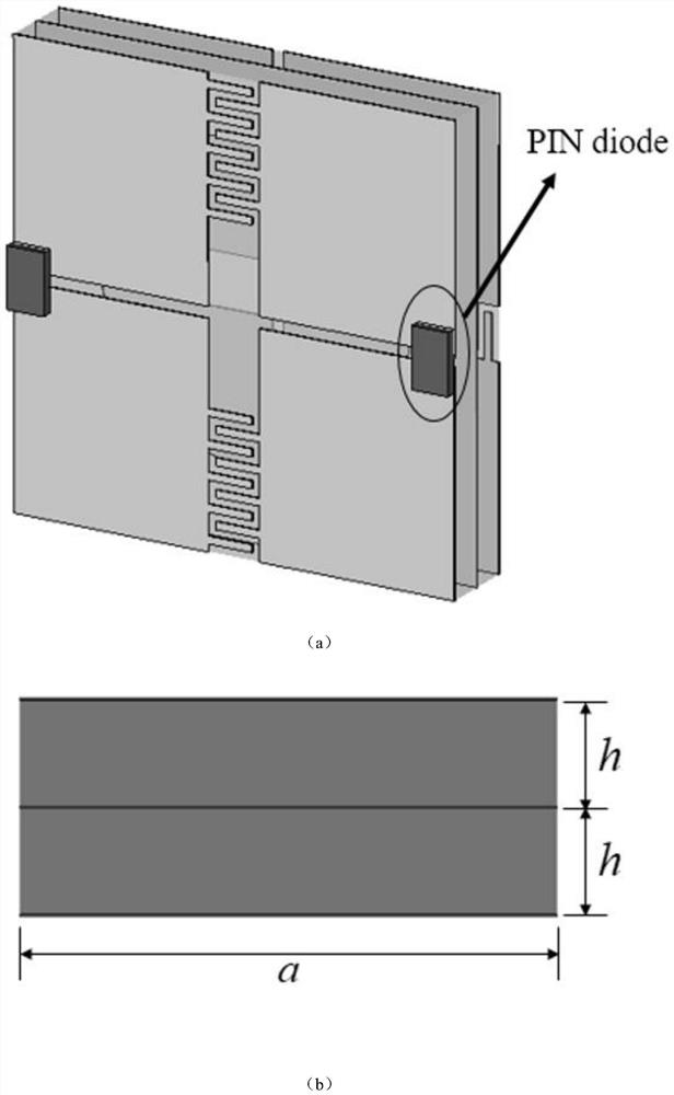
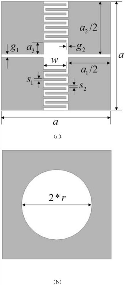
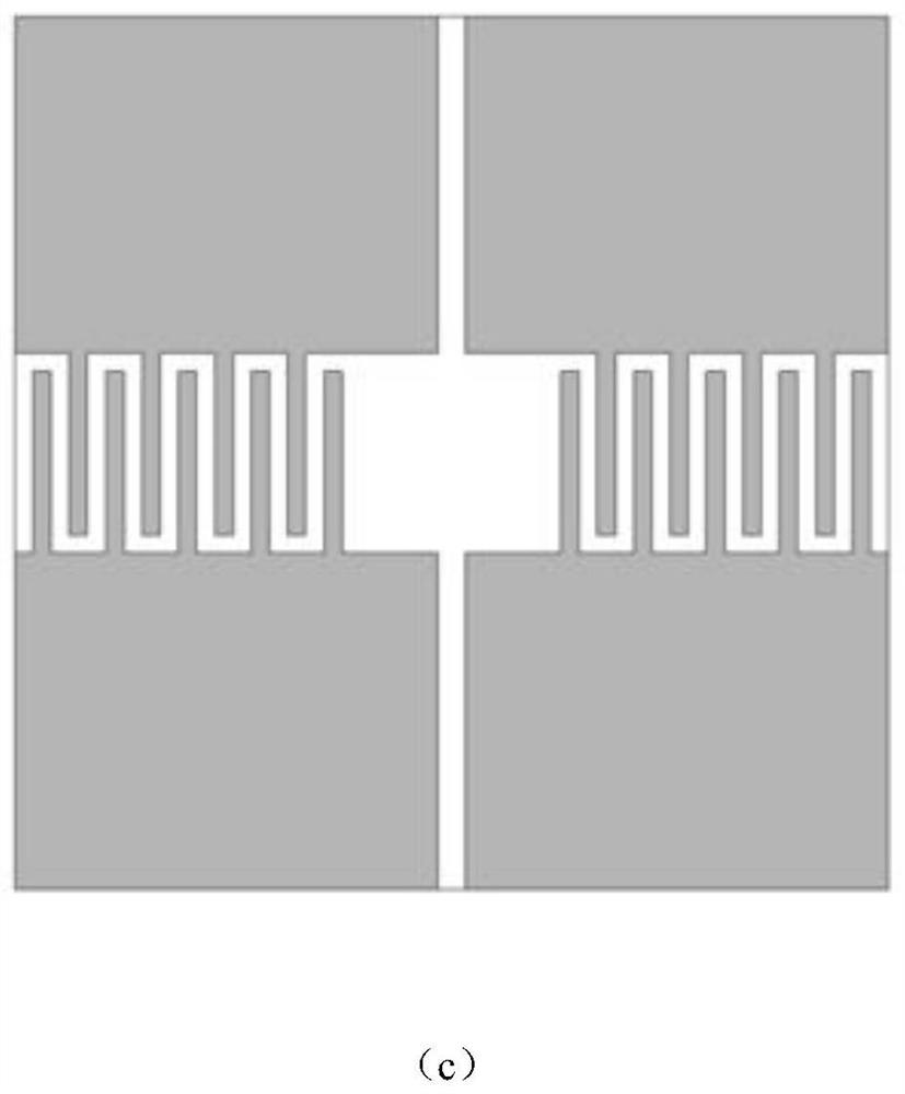
[0049] An X-band ultra-wideband electronically controlled active frequency selective surface based on a PIN diode, the electronically controlled active frequency selective surface unit includes a 3-layer metal plate unit and a 2-layer dielectric plate unit, the 3-layer metal plate unit and 2 The layer dielectric plate units are arranged at intervals, a circular gap is arranged in the center of the middle layer metal plate unit, the upper layer metal plate unit is attached to the upper layer dielectric plate unit, the bottom layer metal plate unit is attached to the lower layer dielectric plate unit, and the vertical direction of the upper layer metal plate unit is A patch slot is arranged, an interdigital capacitor slot is arranged in the lateral direction of the upper metal plate unit, and a square slot is arranged in the center of the upper metal plate unit;
[0050]The upper layer metal plate unit has the same structure as the bottom layer metal plate unit, and the bottom la...
Embodiment 2
[0074] The structure of the electronically controlled active frequency selective surface element is as follows figure 1 As shown, the structure is composed of 3 layers of metal and 2 layers of dielectric. The upper and lower metal layers are mainly square patch structures, and the middle layer metal is a circular slot structure. The dielectric plate material is RogersRT5880, and the relative permittivity ε r is 2.2, and the thickness h of each dielectric plate is 0.508mm. The structure of each layer of metal units is as follows figure 2 As shown in the figure, the metal unit structures of the top layer and the bottom layer are exactly the same, except that they are rotated 90 degrees, and the directions of the PIN diodes loaded on the top layer and the bottom layer are perpendicular to each other. The values of each parameter in the figure are shown in Table 1.
[0075] Table 1 Structural parameters of electronically controlled active frequency selective surface elements ...
PUM
| Property | Measurement | Unit |
|---|---|---|
| width | aaaaa | aaaaa |
| width | aaaaa | aaaaa |
| thickness | aaaaa | aaaaa |
Abstract
Description
Claims
Application Information
 - R&D
- Intellectual Property
- Life Sciences
- Materials
- Tech Scout
- Unparalleled Data Quality
- Higher Quality Content
- 60% Fewer Hallucinations
Browse by: Latest US Patents, China's latest patents, Technical Efficacy Thesaurus, Application Domain, Technology Topic, Popular Technical Reports.
© 2025 PatSnap. All rights reserved.Legal|Privacy policy|Modern Slavery Act Transparency Statement|Sitemap|About US| Contact US: help@patsnap.com


