Circuit board double-chip centering anti-vibration reinforcing structure and controller circuit board
A technology for strengthening structures and circuit boards, applied in printed circuit parts, printed circuit stress/deformation reduction, printed circuits connected with non-printed electrical components, etc. The effect of suppressing the deformation of the board, improving the structure, and reducing the stress
- Summary
- Abstract
- Description
- Claims
- Application Information
AI Technical Summary
Problems solved by technology
Method used
Image
Examples
Embodiment 1
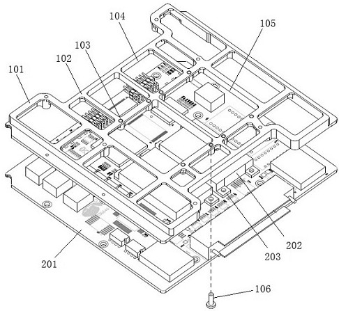
[0035] Embodiment 1: A circuit board double-chip centered anti-seismic strengthening structure, such as figure 1 As shown, it includes a first H-shaped frame 101 and a second H-shaped frame 102 on the same plane, and the second H-shaped frame 102 is arranged in the first H-shaped frame 101 as a beam of the first H-shaped frame 101; the first H The laying directions of the frame 101 and the second H-frame 102 are perpendicular to each other; the two open ends of the first H-frame 101 and the corresponding edge beams of the second H-frame 102 form two centered distributions for the first chip and the second chip. The two chips correspond to the installed reinforcing frame 105 . In this embodiment, the material of the anti-seismic strengthening structure is AL7075 with better strength.
[0036] The edge beams of the first H-shaped frame 101 and the second H-shaped frame 102 are combined by a plurality of closed frames 104 in a linear distribution manner.
[0037] The edge of th...
Embodiment 2
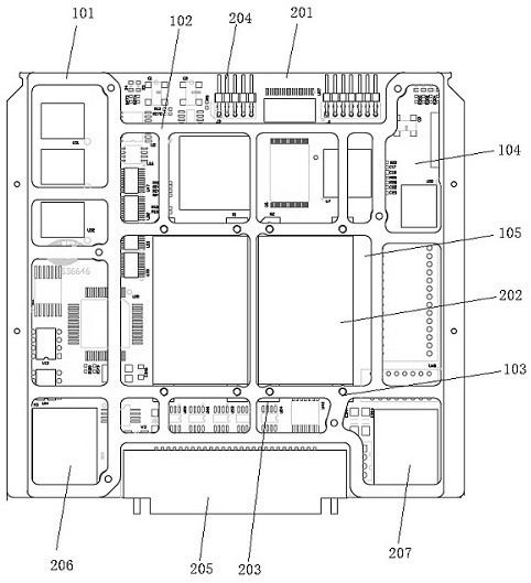
[0039] Embodiment 2: a kind of controller circuit board, such as figure 2 As shown, it includes a PCB board 201 and a circuit board double-chip centered anti-seismic strengthening structure as described in Embodiment 1. The PCB board 201 is equipped with a first chip and a second chip that cooperate with two reinforcing frames 105 .
[0040] Mounting ears 203 corresponding to the threaded through holes 103 are provided on the sides of the first chip and the second chip, and the screws 106 pass through the PCB board 201 and the mounting ears 203 in sequence and are fixedly connected to the threaded through holes 103 .
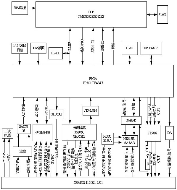
[0041] Such as figure 2 and image 3As shown, PCB board 201 is also installed with DSP module, FPGA module, resolver excitation module, photoelectric isolation module, power supply module, AD acquisition module, DA output module, JTAG interface device 204, ZRM connector 205, operational amplifier module, power Oscillating module; the first chip and the secon...
PUM
 Abstract
Description
Claims
Application Information
 - Generate Ideas
- Intellectual Property
- Life Sciences
- Materials
- Tech Scout
- Unparalleled Data Quality
- Higher Quality Content
- 60% Fewer Hallucinations
Browse by: Latest US Patents, China's latest patents, Technical Efficacy Thesaurus, Application Domain, Technology Topic, Popular Technical Reports.
© 2025 PatSnap. All rights reserved.Legal|Privacy policy|Modern Slavery Act Transparency Statement|Sitemap|About US| Contact US: help@patsnap.com


