Combined growth system with multiple epitaxial reaction chambers, operation method, equipment, manufactured chip and application thereof

An operation method and reaction chamber technology, applied in semiconductor/solid-state device manufacturing, coating, gaseous chemical plating, etc., can solve the problems of increased time cost, non-compliance, capacity matching, etc., to reduce equipment and time, design Reasonable and convenient, with wide application prospects

Active Publication Date: 2022-01-25
FOSHAN UNIVERSITY
View PDF0 Cites 0 Cited by
  • Summary
  • Abstract
  • Description
  • Claims
  • Application Information

AI Technical Summary

Problems solved by technology

However, the existing preparation process is a segmented process. The design and manufacture of the mainstream MOCVD machines on the market at present determine that equipment users have to manually repeat the feeding and discharging of epitaxial wafers for more than 2 times for each complete production round of LED chips. In this way, the growth efficiency of the product is severely limited. There is a huge difference in the growth atmosphere during the integration of nitride MOCVD (reducing atmosphere) and oxide MOCVD (oxidizing atmosphere), and there are problems such as capacity matching. The main reasons are: III- The preparation time of group V compound epitaxial wafers (generally 6~7H, depending on the actual process) is quite different from the growth time of II-VI compound epitaxial wafers (generally 2H, depending on the actual process) , which will undoubtedly increase various costs such as time, which will easily affect production efficiency, and also does not conform to the concept of modern automation and green energy saving
In addition, because it is impossible to achieve multiple types of one machine, it is still necessary to use a segmented process, and use a single MOCVD machine corresponding to different functions to prepare different layers of materials or films
[0005] In fact, the monolithic MOCVD machines used in the processing of different functional materials or thin films are relatively similar in structure. Therefore, if problems such as capacity matching are to be overcome, multiple epitaxial wafers for the preparation of III-V compounds may be required. The MOCVD machine is used in conjunction with a single MOCVD machine used to prepare II-VI compound epitaxial wafers, and to prepare blue LED chips. However, in this way, multiple MOCVD machines need to be put into use, which undoubtedly greatly increases the cost of the equipment. It also brings huge initial high cost investment and invisible pressure to production, and it also does not conform to the concept of modern automation and green energy saving

Method used


Image

  • Combined growth system with multiple epitaxial reaction chambers, operation method, equipment, manufactured chip and application thereof
  • Combined growth system with multiple epitaxial reaction chambers, operation method, equipment, manufactured chip and application thereof
  • Combined growth system with multiple epitaxial reaction chambers, operation method, equipment, manufactured chip and application thereof

Examples


Embodiment 1

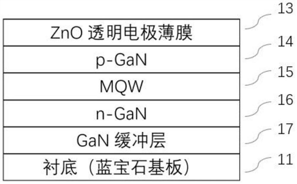
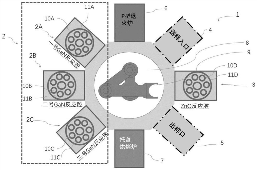
[0057] The first MOCVD machine for producing GaN epitaxial wafers and the second MOCVD machine for producing ZnO thin films are used, and the growth time of GaN epitaxial growth is set to 6h, and the growth time of ZnO thin film is set to 2.5h (=preheating time length 0.5h+actual The growth time is 2h), then the number of GaN reaction chambers is 6 / 2.5=2.4, take 3, and the number of ZnO reaction chambers is 1, connected to production, such as figure 2 shown.

[0058] The epitaxial joint growth process of this embodiment is:

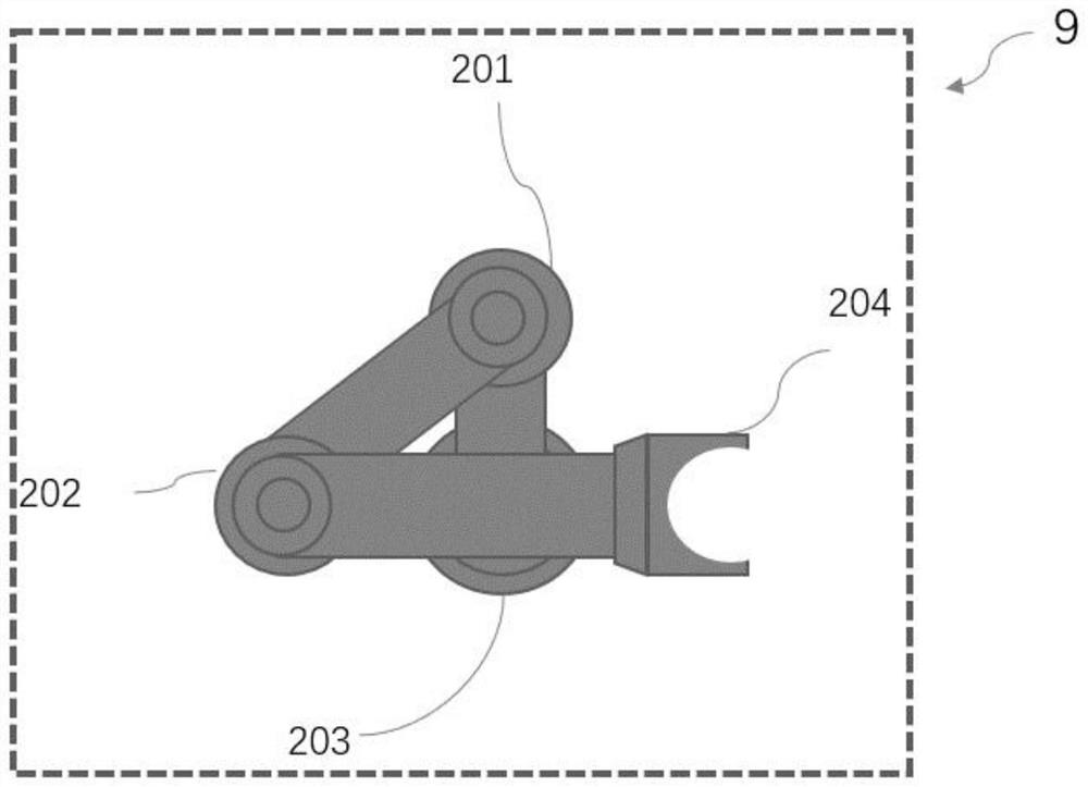
[0059] 1) Put the graphite disk 11 with the substrate 10 into the sample delivery inlet 4, close the external entrance of the sample delivery inlet 4, open the interface with the transfer box 8, and the transmission arm 9 sends the graphite disk 11 with the substrate 10 to the The transmission box 8, the interface between the sample delivery inlet 4 and the transmission box 8 is closed, the transmission box 8 starts to extract air to create a vacuum env...


PUM


Abstract

The invention belongs to the technical field of production and preparation of semiconductor materials, and discloses a combined growth system with a plurality of epitaxial reaction chambers, an operation method, equipment, manufactured chips and applications thereof. Use a dedicated MOCVD machine to sequentially grow III-V compound epitaxial wafers and II-VI compound epitaxial wafers on the substrate, and set a number of III-V compound reaction chambers to start sequentially. The growth time y of the group VI compound epitaxial wafer is equal, and the multi-cavity sub-step is adopted, which not only makes the III-V group compound and the II-VI group compound are deposited more effectively in the reaction chamber respectively, but also realizes time-sharing multiplexing. Effective integration and capacity matching of application and segmented processes. At the same time, it also provides an epitaxial joint growth equipment with multiple reaction chambers, including a first growth device, a pushing device and a second growing device, and a transmission arm is arranged in the pushing device. The invention achieves the maximum utilization of the MOCVD machine and each reaction chamber under the condition of ensuring continuous production, and has wide application prospects.

Description

technical field [0001] The invention belongs to the technical field of production and preparation of semiconductor materials, and in particular relates to a combined growth system with multiple epitaxial reaction chambers, an operation method, equipment, manufactured chips and applications thereof. Background technique [0002] Epitaxial wafers of II-VI compounds (such as ZnO transparent electrode films, etc.) are transparent in the wavelength range of 400nm~2μm, so they can be used to make transparent electrodes. Doping the II-VI group compound with a small amount of Al and Ga can obtain a low-resistance, high-transmittance and high-quality II-VI group compound film, which can be used as a current spreading layer. In addition, the II-VI compound transparent electrode film also has the advantages of non-toxicity, low cost, environmental friendliness, and relative stability at high temperature, and is known as the preferred transparent electrode material to replace ITO materi...

Claims


Application Information

Patent Timeline
Patent Type & Authority Patents(China)
IPC IPC(8): C23C16/54C23C16/52C23C16/40C23C16/56C23C16/34H01L21/67H01L33/00
CPCC23C16/54C23C16/52C23C16/303C23C16/407C23C16/56H01L21/67155H01L33/005H01L33/007H01L33/42H01L33/32H01L2933/0016H01L33/0095C30B29/00H01L25/0753
Inventor 范冰丰洪泽楷陈国杰
Owner FOSHAN UNIVERSITY
Why Eureka
Try Eureka