Manufacturing method of high-dielectric-constant metal gate

A technology with high dielectric constant and manufacturing method, which is applied in semiconductor/solid-state device manufacturing, circuits, electrical components, etc., can solve the problems of side wall and top sealing, Al cannot be filled in, Al holes, etc., to prevent sealing and prevent Hole, Performance Guaranteed Effect

Active Publication Date: 2021-01-29
SHANGHAI HUALI INTEGRATED CIRCUTE MFG CO LTD
View PDF5 Cites 0 Cited by
  • Summary
  • Abstract
  • Description
  • Claims
  • Application Information

AI Technical Summary

Problems solved by technology

Since PMOS, that is, PFET, has an extra layer of P-type work function layer TiN film, the aspect ratio becomes very large during subsequent filling, which can easily lead to sidewall and top overhang effects, resulting in the failure of subsequent Al filling, resulting in Al hole

Method used


Image

  • Manufacturing method of high-dielectric-constant metal gate
  • Manufacturing method of high-dielectric-constant metal gate
  • Manufacturing method of high-dielectric-constant metal gate

Examples


Embodiment Construction

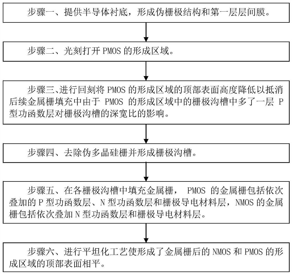
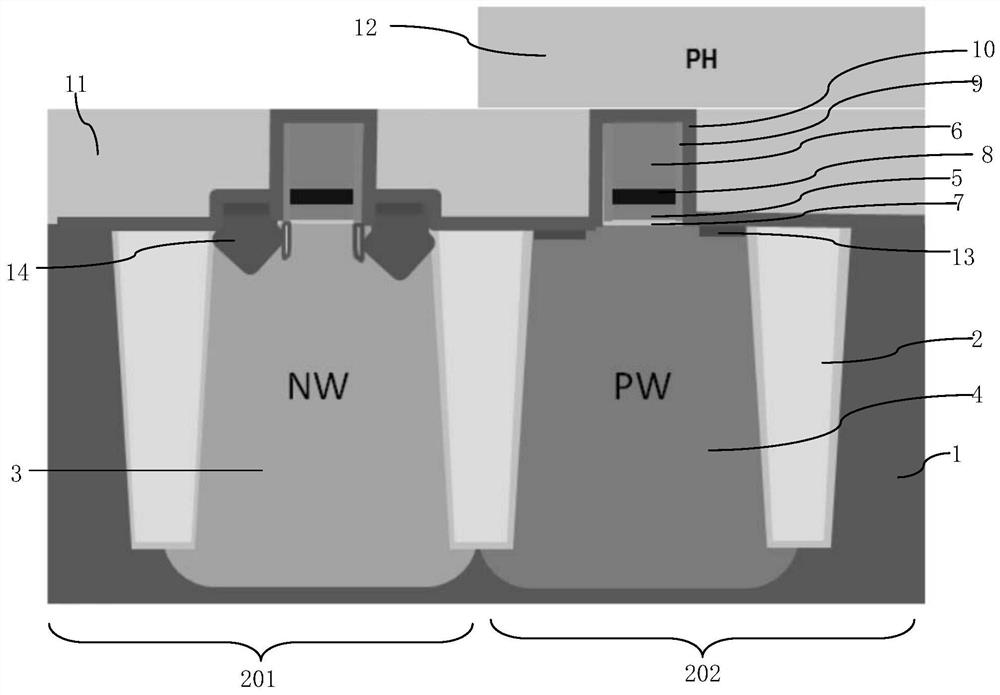
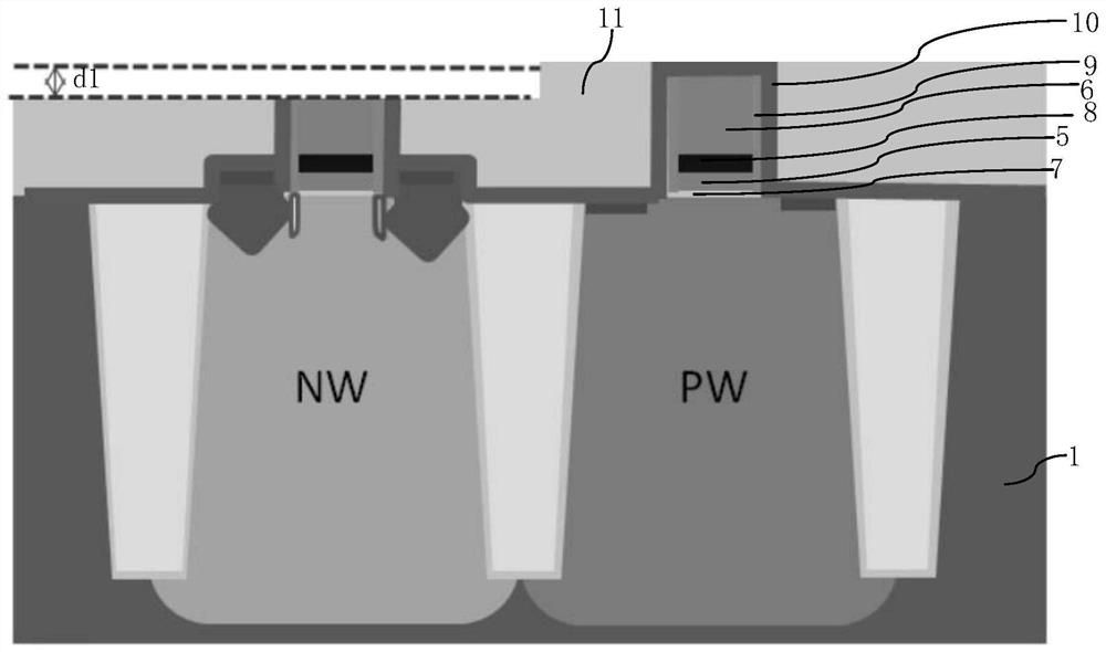
[0044] Such as figure 1 Shown is the flow chart of the manufacturing method of the high dielectric constant metal gate of the embodiment of the present invention; as Figure 2A to Figure 2E Shown is a device structure diagram in each step of the manufacturing method of the high dielectric constant metal gate of the embodiment of the present invention; the manufacturing method of the high dielectric constant metal gate of the embodiment of the present invention includes the following steps:

[0045] Step one, such as Figure 2A As shown, a semiconductor substrate 1 is provided, and the semiconductor substrate 1 includes an NMOS formation region 202 and a PMOS formation region 201 .

[0046] A dummy gate structure and a first interlayer film 11 are formed on the semiconductor substrate 1 and planarized for the first time. The dummy gate structure includes a gate dielectric layer and a dummy polysilicon gate 6 stacked in sequence.

[0047]Both the NMOS forming region 202 and th...


PUM


Abstract

The invention discloses a method for manufacturing a high-dielectric-constant metal gate, which comprises the following steps of: 1, providing a semiconductor substrate, and forming a pseudo gate structure and a first interlayer film; 2, photoetching to open a PMOS formation region; 3, performing back etching to reduce the height of the top surface of the PMOS formation region so as to counteractthe influence of one more P-type work function layer in the gate trench in the PMOS formation region on the depth-to-width ratio of the gate trench in subsequent metal gate filling; 4, removing the pseudo polysilicon gate and forming a gate trench; 5, filling each gate trench with a metal gate, the metal gate of the PMOS comprising a P-type work function layer, an N-type work function layer and agate conductive material layer which are stacked in sequence, and the metal gate of the NMOS comprising an N-type work function layer and a gate conductive material layer which are stacked in sequence; and 6, carrying out a second planarization process to enable the top surfaces of the NMOS and PMOS forming regions on which the metal gates are formed to be flush with each other. According to the invention, the filling process window and the filling quality of the metal gate of the PMOS can be improved.

Description

technical field [0001] The invention relates to a method for manufacturing a semiconductor integrated circuit, in particular to a method for manufacturing a high dielectric constant metal gate (HKMG). Background technique [0002] With the development of CMOS technology, traditional silicon dioxide gate dielectric and polysilicon gate (Poly SiON) transistors have reached physical limits, such as the problem of excessive leakage current due to quantum tunneling effect and the depletion of polysilicon gate problems, etc. seriously affect the performance of semiconductor devices. Starting from the 45nm technology node, the HKMG stacked transistor developed on the basis of the HKMG process effectively solves the above technical problems. [0003] The applicant has adopted the mainstream metal gate-last (Gate-Last) deposition and front-gate dielectric (HK-First) deposition processes in the industry at the 28nm high dielectric constant metal gate technology node. In this process...

Claims


Application Information

Patent Timeline
Patent Type & Authority Applications(China)
IPC IPC(8): H01L21/8238
CPCH01L21/823842
Inventor 于嫚史志界林宗模
Owner SHANGHAI HUALI INTEGRATED CIRCUTE MFG CO LTD
Why Eureka
Try Eureka