


Quick Research
Generate reliable direction feasibility study reports for your R&D in just a few steps.

Technical Q&A
Discover and master advanced knowledge NOW. Basics, ideas, possibilities, all at once.

Find Solutions
As an expert in R&D theories, this can generate solutions to your technical problems instantly.

Evaluate Feasibility
Analyze your overall solution with one click, know your potential R&D risks in advance.

Monitor Landscape
Get weekly tech updates, stay abreast of the latest tech innovations and key insights.
Semiconductor tester communication bus system
A technology of communication bus and testing machine, which is applied in the field of high-bandwidth and strong real-time semiconductor testing machine communication bus system, can solve the problems that the transmission bus cannot guarantee the delay and accuracy of data transmission, and cannot guarantee high-precision synchronization requirements, etc., to meet the requirements of Strong real-time access requirements, improve system load capacity, and meet large-scale effects
- Summary
- Abstract
- Description
- Claims
- Application Information
AI Technical Summary
Problems solved by technology
Method used
Image

Examples
Embodiment Construction
[0028] In order to make the object, technical solution and advantages of the present invention clearer, the present invention will be described in detail below in conjunction with the accompanying drawings and specific embodiments.
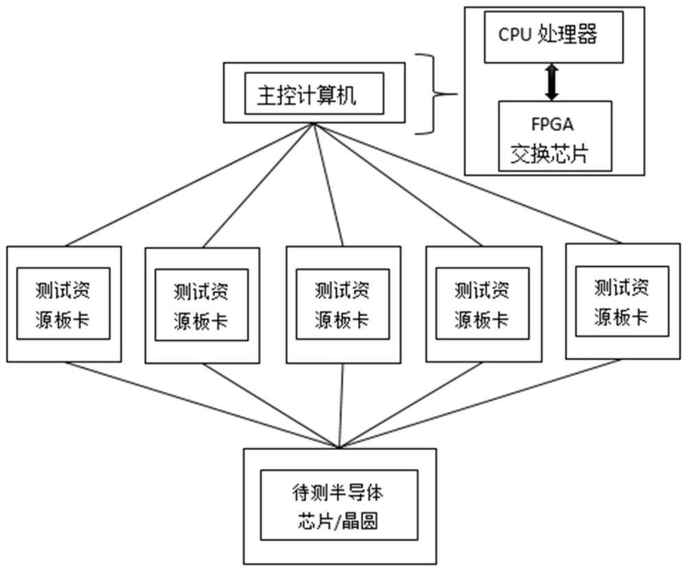
[0029] Such as figure 1 In the shown embodiment of the present invention, the semiconductor testing machine communication bus system of the present invention is shown, including a main control computer connected through an interface bus and more than one test resource board, the main control computer is used to run a specific test program, control Each test resource board outputs excitation signals to the semiconductor chip / wafer to be tested and measures the feedback signal of the semiconductor chip / wafer to be tested, and determines the quality of the chip / wafer by judging the consistency between the feedback signal and the expected result. The central processing unit of the main control computer is connected to a high-performance FPGA switching...
PUM
 Abstract
Description
Claims
Application Information
 - R&D Engineer
- R&D Manager
- IP Professional
- Industry Leading Data Capabilities
- Powerful AI technology
- Patent DNA Extraction
Browse by: Latest US Patents, China's latest patents, Technical Efficacy Thesaurus, Application Domain, Technology Topic, Popular Technical Reports.
© 2024 PatSnap. All rights reserved.Legal|Privacy policy|Modern Slavery Act Transparency Statement|Sitemap|About US| Contact US: help@patsnap.com