Rewiring layer and preparation method thereof

A technology of rewiring layer and seed layer, applied in semiconductor/solid-state device manufacturing, electrical components, electrical solid-state devices, etc., can solve the problem of easy peeling of fine-pitch rewiring layers, and achieve the effect of preventing peeling and reducing side erosion.

Pending Publication Date: 2021-01-22
SJ SEMICON JIANGYIN CORP
View PDF0 Cites 1 Cited by
  • Summary
  • Abstract
  • Description
  • Claims
  • Application Information

AI Technical Summary

Problems solved by technology

[0005] In view of the above-mentioned shortcomings of the prior art, the purpose of the present invention is to propose a rewiring layer and a preparation method for solving the problem that the fine-pitch rewiring layer is easy to peel off

Method used


Image

  • Rewiring layer and preparation method thereof
  • Rewiring layer and preparation method thereof
  • Rewiring layer and preparation method thereof

Examples


Embodiment 1

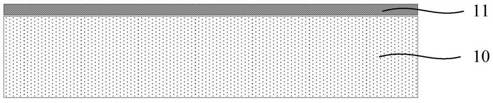
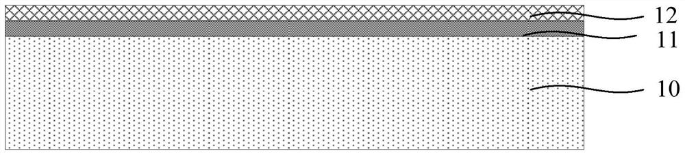
[0048] Such as Figure 1-9 As shown, this embodiment provides a rewiring and a method for preparing a rewiring layer.

[0049] Such as Figure 9 As shown, the rewiring layer at least includes: a metal seed layer 12 , a metal wire layer 14 located on the upper surface of the metal seed layer 11 , and a plastic encapsulation layer 15 covering the upper surfaces and side walls of the metal seed layer 12 and the metal wire layer 14 .

[0050] The material of the metal seed layer 12 is copper or aluminum, but must be a single material. This is because wet etching is one of the important procedures for the preparation process of the rewiring layer, and the etchant has different etching rates for different metals. If two or more metals are used to prepare the metal seed layer, multiple wet etching is required, and due to the isotropy of etching, it will cause side etching, thereby reducing the connection area between the metal line layer and the substrate. This leads to the peelin...

Embodiment 2

[0082] This embodiment provides a method for preparing a rewiring layer.

[0083] This embodiment adopts a process similar to that of Embodiment 1. The difference from Embodiment 1 is that the materials of the metal seed layer and the metal wire layer in this embodiment are the same, and copper is used as the metal seed layer and the metal wire layer. .

[0084] Other structures and processes are the same as those in Embodiment 1, and will not be repeated here.

[0085] In this embodiment, the metal line layer and the metal seed layer are made of the same and single material. During the preparation process of the rewiring layer, the side etching phenomenon caused by the isotropy of wet etching can be reduced, thereby improving the rewiring layer. Fabrication yield of the wiring layer.

[0086] In summary, the present invention provides a rewiring layer and a preparation method thereof. The rewiring layer includes: a metal seed layer; a metal wire layer located on the upper s...


PUM


Abstract

The invention provides a rewiring layer and a preparation method thereof. The rewiring layer comprises a metal seed layer, a metal wire layer which is positioned on the upper surface of the metal seedlayer, and a plastic package layer which covers the upper surfaces and the side walls of the metal wire layer and the metal seed layer. The metal seed layer is made of a single material. The metal seed layer made of a single material is adopted to replace a traditional Ti / Cu seed layer, so that side etching caused by a wet etching process is reduced, stripping of the rewiring layer caused by reduction of a connecting surface between the metal wire layer and the substrate is prevented, the etching process is reduced, and the yield of the fine-pitch rewiring layer is improved.

Description

technical field [0001] The invention relates to the field of semiconductor technology packaging, in particular to a rewiring layer and a preparation method thereof. Background technique [0002] With the trend of multi-function and miniaturization of electronic products, high-density microelectronic assembly technology has gradually become the mainstream in the new generation of electronic products. In order to cope with the development of a new generation of electronic products, especially the development of smart phones, PDAs, ultrabooks and other products, the size of chips is developing in the direction of higher density, faster speed, smaller size, and lower cost. The emergence of fan-out wafer-level packaging technology provides a broader development prospect for the improvement of technology. [0003] For high I / O (input / output) chip packaging structures, multiple layers of rewiring are required to achieve high density interposers. However, under the limited shape a...

Claims


Application Information

Patent Timeline
Patent Type & Authority Applications(China)
IPC IPC(8): H01L21/60H01L23/482H01L21/683
CPCH01L21/6835H01L24/02H01L24/03H01L2221/68359H01L2224/0231H01L2224/02315H01L2224/02381H01L2224/03
Inventor 尹佳山周祖源吴政达林正忠
Owner SJ SEMICON JIANGYIN CORP
Why Eureka
Try Eureka