
Shifting register and driving method thereof, grid driving circuit, display panel and device

A shift register and frequency display technology, which is applied in the fields of display panels and devices, shift registers and driving methods, and gate drive circuits, can solve the problems of long data update period, affecting display effect, and large PMOS leakage current, etc., to achieve Guarantee normal display effect

Active Publication Date: 2021-01-22
WUHAN TIANMA MICRO ELECTRONICS CO LTD
View PDF17 Cites 9 Cited by
  • Summary
  • Abstract
  • Description
  • Claims
  • Application Information

AI Technical Summary

Problems solved by technology

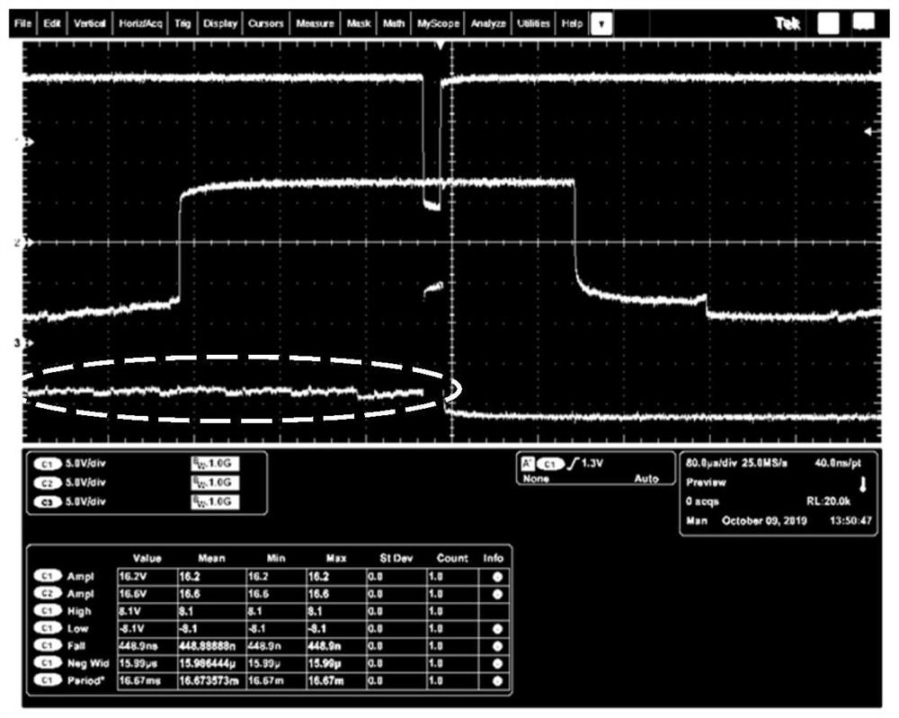
However, due to the large leakage current of the PMOS formed by the low temperature polysilicon (Low Temperature Poly-Silicon, LTPS) material, the data update period is longer when driving at a low frame rate. When there is a leakage current in the shift register circuit, the shift register circuit The bit register circuit cannot output a stable control signal, causing the display screen of the display device to flicker, affecting the display effect

Method used


Image

  • Shifting register and driving method thereof, grid driving circuit, display panel and device
  • Shifting register and driving method thereof, grid driving circuit, display panel and device
  • Shifting register and driving method thereof, grid driving circuit, display panel and device

Examples


Embodiment Construction

[0038] The present invention will be further described in detail below in conjunction with the accompanying drawings and embodiments. It should be understood that the specific embodiments described here are only used to explain the present invention, but not to limit the present invention. In addition, it should be noted that, for the convenience of description, only some structures related to the present invention are shown in the drawings but not all structures.

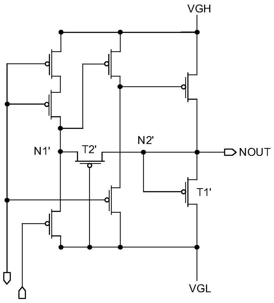
[0039] figure 1 It is a partial circuit schematic diagram of a shift register in the related art, which shows a shift register of a PMOS design, such as figure 1 As shown, in the shift register circuit, the gate of the first transistor T1' that controls the output scan N is connected to the higher potential N1' node through the second transistor T2', because the second transistor T2' has a certain leakage current, so When driving at low frequency, due to the low refresh rate of the display, the scan N needs to be...


PUM


Abstract

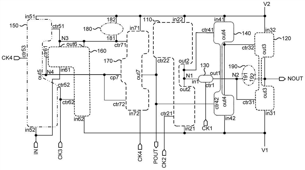
The invention discloses a shift register and a driving method thereof, a gate driving circuit, a display panel and a device. The shift register comprises a first power supply signal input end, a second power supply signal input end, a first signal output end, a first node control module, a first output module, a first voltage stabilizing module and a first clock signal end; the first end of the first voltage stabilizing module is electrically connected with the output end of the first node control module at a first node, the second end of the first voltage stabilizing module is electrically connected with the first control end of the first output module at a second node, and the control end of the first voltage stabilizing module is electrically connected with a first clock signal end; andin the high-frequency display stage, and the first voltage stabilization control module is conducted, and in the low-frequency display stage, the first voltage stabilization control module is conducted or cut off. By additionally arranging the first voltage stabilizing module and the first clock signal end, due to the fact that the leakage current of the first voltage stabilizing module is small,the leakage current of the second node can be reduced in the low-frequency display stage, and stable output of the first signal output end is maintained.

Description

technical field [0001] Embodiments of the present invention relate to the field of display technology, and in particular to a shift register and a driving method, a gate driving circuit, a display panel and a device. Background technique [0002] With the development of display technology, while pursuing a higher resolution of the display device, the power consumption of the display device increases accordingly. In order to reduce power consumption of a display device, a frame rate may be reduced to drive pixels at a low speed during a certain period of time. For example, in a mobile terminal, the normal display mode executes a normal driving frequency based on 60 Hz or 120 Hz; in the standby mode, executes a driving frequency based on 1 Hz-5 Hz, thus reducing power consumption. [0003] In the prior art, a P-type Metal Oxide Semiconductor Field Effect Transistor (Positive Channel Metal Oxide Semiconductor, PMOS) design is mostly used in the shift register circuit. However...

Claims


Application Information

Patent Timeline
Patent Type & Authority Applications(China)
IPC IPC(8): G09G3/20G11C19/28
CPCG09G3/20G11C19/28G09G2310/0286G09G3/3266G09G2320/0214G09G2320/0247G09G3/3258G09G3/3655G09G3/3677G09G2310/08
Inventor 张蒙蒙周星耀
Owner WUHAN TIANMA MICRO ELECTRONICS CO LTD
Learn More