Photoelectrode and preparation method and application thereof
A photoelectrode and electrode technology, applied in the photoelectrode field, can solve the problems of photocorrosion, high cost of precious metals, and limited large-scale application, and achieve the effects of improved performance, improved efficiency, and improved photocatalytic performance and activity.
- Summary
- Abstract
- Description
- Claims
- Application Information
AI Technical Summary
Problems solved by technology
Method used
Image
Examples
Embodiment 1
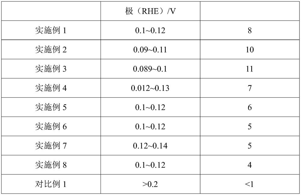
[0073] This embodiment provides a kind of photoelectrode, described photoelectrode comprises fluorine-doped tin dioxide glass carrier and functional layer, and described functional layer comprises cuprous oxide thin film layer, cuprous sulfide thin film layer and Mo 2 CT x film layer. Among them, cuprous oxide thin film layer, cuprous sulfide thin film layer and Mo 2 CT x The thin film layers are sequentially stacked on the fluorine-doped tin dioxide glass carrier; the cuprous oxide thin film layer is located on the surface of the fluorine-doped tin dioxide glass carrier;
[0074] Described cuprous oxide film layer, cuprous sulfide film layer and Mo 2 The mass ratio of the CTx thin film layer is 1:0.17:0.1.
[0075] The preparation method of the photoelectrode is as follows:
[0076] (1) Prepare 0.05mol of Cu S o 4 and 50 mL of a mixed solution of 0.05 mol of trisodium citrate, and then adjust its pH value to 11.0 with 1 mol of NaOH solution, and heat the mixed solution...
Embodiment 2
[0081] This embodiment provides a kind of photoelectrode, described photoelectrode comprises fluorine-doped tin dioxide glass carrier and functional layer, and described functional layer comprises cuprous oxide thin film layer, cuprous sulfide thin film layer and Mo 2 CT x film layer. Among them, cuprous oxide thin film layer, cuprous sulfide thin film layer and Mo 2 CT x The thin film layers are sequentially stacked on the fluorine-doped tin dioxide glass carrier; the cuprous oxide thin film layer is located on the surface of the fluorine-doped tin dioxide glass carrier;
[0082] Described cuprous oxide film layer, cuprous sulfide film layer and Mo 2 CT x The mass ratio of the film layer is 1:0.15:0.1.
[0083] The preparation method of the photoelectrode is as follows:
[0084] (1) Prepare 0.05mol of Cu S o 4 and 50 mL of a mixed solution of 0.05 mol of trisodium citrate, and then adjust its pH value to 10.8 with 1 mol of NaOH solution, and heat the mixed solution to...
Embodiment 3
[0089] This embodiment provides a kind of photoelectrode, described photoelectrode comprises fluorine-doped tin dioxide glass carrier and functional layer, and described functional layer comprises cuprous oxide thin film layer, cuprous sulfide thin film layer and Mo 2 CT x film layer. Among them, cuprous oxide thin film layer, cuprous sulfide thin film layer and Mo 2 CT x The thin film layers are sequentially stacked on the fluorine-doped tin dioxide glass carrier; the cuprous oxide thin film layer is located on the surface of the fluorine-doped tin dioxide glass carrier;
[0090] Described cuprous oxide film layer, cuprous sulfide film layer and Mo 2 CT x The mass ratio of the film layer is 1:0.18:0.12.
[0091] The preparation method of the photoelectrode is as follows:
[0092] (1) Prepare 0.05mol of Cu S o 4 and 50 mL of a mixed solution of trisodium citrate of 0.05 mol, and then adjust its pH value to 11.5 with 1 mol of NaOH solution, and heat the mixed solution t...
PUM
| Property | Measurement | Unit |
|---|---|---|
| thickness | aaaaa | aaaaa |
| thickness | aaaaa | aaaaa |
| thickness | aaaaa | aaaaa |
Abstract
Description
Claims
Application Information
 - R&D Engineer
- R&D Manager
- IP Professional
- Industry Leading Data Capabilities
- Powerful AI technology
- Patent DNA Extraction
Browse by: Latest US Patents, China's latest patents, Technical Efficacy Thesaurus, Application Domain, Technology Topic, Popular Technical Reports.
© 2024 PatSnap. All rights reserved.Legal|Privacy policy|Modern Slavery Act Transparency Statement|Sitemap|About US| Contact US: help@patsnap.com


