Electromagnetic shielding module packaging structure and electromagnetic shielding module packaging method

A technology of electromagnetic shielding and packaging structure, applied in circuits, electrical components, electrical solid devices, etc., can solve the problems of increasing the design space of the substrate surface, unfavorable device miniaturization, and unfavorable high-efficiency placement, avoiding the problem of glue overflow, and facilitating The effect of miniaturization and reduction of design space

Active Publication Date: 2021-02-26
FOREHOPE ELECTRONICS NINGBO CO LTD
View PDF7 Cites 0 Cited by
  • Summary
  • Abstract
  • Description
  • Claims
  • Application Information

AI Technical Summary

Problems solved by technology

[0002] The existing electromagnetic shielding packaging structure usually achieves the electromagnetic shielding function by directly bonding wires around the chip on the substrate to form metal pillars, and then dispensing glue to fix it. However, directly bonding wires on the substrate will cause the entire mounting process to be cumbersome. does not utilize high-efficiency placement
At the same time, glue dispensing is also likely to cause glue overflow. The glue overflows to the pad area, causing chip failure, and the metal pillars also greatly increase the design space on the substrate surface, increasing the overall thickness, which is not conducive to the miniaturization of the device.

Method used


Image

  • Electromagnetic shielding module packaging structure and electromagnetic shielding module packaging method
  • Electromagnetic shielding module packaging structure and electromagnetic shielding module packaging method
  • Electromagnetic shielding module packaging structure and electromagnetic shielding module packaging method

Examples


no. 1 example

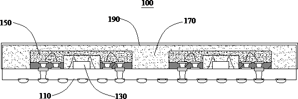
[0045] Please refer to Figure 1 to Figure 3, this embodiment provides an electromagnetic shielding module packaging structure 100, which has a good electromagnetic shielding effect and can avoid the problem of glue overflow caused by dispensing, and the assembly process is simple, the efficiency is high, and the design space of the substrate surface is small, reducing the cost of components. Thickness is conducive to the miniaturization of devices.

[0046] The electromagnetic shielding module packaging structure 100 provided in this embodiment includes a module substrate 110, a chip 130, a partition shielding device 150, a protective plastic package 170, and a metal shielding layer 190. The chip 130 is mounted on the module substrate 110, and the partition shielding The device 150 is mounted on the module substrate 110 and covered outside the chip 130. The protective plastic package 170 is arranged on the module substrate 110 and covered outside the partition shielding devic...

no. 2 example

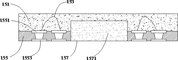
[0061] See Figure 4 and Figure 5 , this embodiment provides an electromagnetic shielding module packaging structure 100, its basic structure and principle and the technical effects produced are the same as those of the first embodiment, for a brief description, for the part not mentioned in this embodiment, please refer to the first Corresponding content in an embodiment.

[0062] The electromagnetic shielding module packaging structure 100 provided in this embodiment includes a module substrate 110, a chip 130, a partition shielding device 150, a protective plastic package 170, and a metal shielding layer 190. The chip 130 is mounted on the module substrate 110, and the partition shielding The device 150 is mounted on the module substrate 110 and covered outside the chip 130. The protective plastic package 170 is arranged on the module substrate 110 and covered outside the partition shielding device 150. The metal shielding layer 190 is covered on the protective plastic pa...

no. 3 example

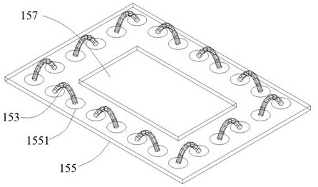
[0068] See Figure 6 to Figure 8 , this embodiment provides an electromagnetic shielding module packaging structure 100, its basic structure and principle and the technical effects produced are the same as those of the first embodiment, for a brief description, for the part not mentioned in this embodiment, please refer to the first Corresponding content in an embodiment.

[0069] In this embodiment, the electromagnetic shielding module packaging structure 100 includes a module substrate 110, a chip 130, a partition shielding device 150, a protective plastic package 170, and a metal shielding layer 190. The chip 130 is mounted on the module substrate 110, and the partition shielding The device 150 is mounted on the module substrate 110 and covered outside the chip 130. The protective plastic package 170 is arranged on the module substrate 110 and covered outside the partition shielding device 150. The metal shielding layer 190 is covered on the protective plastic package. 170...


PUM


Abstract

Embodiments of the present invention provide an electromagnetic shielding module packaging structure and an electromagnetic shielding module packaging method, which relate to the technical field of semiconductor packaging. The electromagnetic shielding module packaging structure includes a module substrate, a chip, a partitioned shielding device, and a protective plastic body. And the metal shielding layer, the partition shielding device includes a shielding plastic package and a plurality of conductive arcs arranged in the shielding plastic package, electromagnetic shielding is realized by setting the partition shielding device, no need to dispense glue, and at the same time, the plastic package is opened for accommodating chips. By giving way to the groove, and by implementing the electromagnetic shielding function in the plurality of conductive arcs, the conductive arcs can be made lower than the prior art, thereby reducing the design space of the substrate surface. Compared with the prior art, the electromagnetic shielding module package structure provided by the present invention can avoid the problem of glue overflow caused by glue dispensing, and has a simple assembly process, high efficiency, and a small design space on the surface of the substrate, which reduces the thickness of the device, and has advantages. Conducive to the miniaturization of devices.

Description

technical field [0001] The invention relates to the technical field of semiconductor packaging, in particular to an electromagnetic shielding module packaging structure and an electromagnetic shielding module packaging method. Background technique [0002] The existing electromagnetic shielding packaging structure usually achieves the electromagnetic shielding function by directly bonding wires around the chip on the substrate to form metal pillars, and then dispensing glue to fix it. However, directly bonding wires on the substrate will cause the entire mounting process to be cumbersome. High-efficiency placement is not utilized. At the same time, glue dispensing can also easily cause glue overflow. The glue overflows to the pad area, causing chip failure, and the metal pillars also greatly increase the design space on the substrate surface, increasing the overall thickness, which is not conducive to the miniaturization of the device. Contents of the invention [0003] T...

Claims


Application Information

Patent Timeline
Patent Type & Authority Patents(China)
IPC IPC(8): H01L23/552H01L23/31H01L21/50H01L21/56
CPCH01L21/50H01L21/561H01L23/3107H01L23/552H01L2224/48091H01L2924/181H01L2924/19107H01L2924/00012H01L2924/00014
Inventor 徐玉鹏何正鸿
Owner FOREHOPE ELECTRONICS NINGBO CO LTD
Why Eureka
Try Eureka