


Quick Research
Generate reliable direction feasibility study reports for your R&D in just a few steps.

Technical Q&A
Discover and master advanced knowledge NOW. Basics, ideas, possibilities, all at once.

Find Solutions
As an expert in R&D theories, this can generate solutions to your technical problems instantly.

Evaluate Feasibility
Analyze your overall solution with one click, know your potential R&D risks in advance.

Monitor Landscape
Get weekly tech updates, stay abreast of the latest tech innovations and key insights.
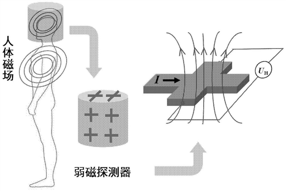
Method for carrying out low-intensity magnetic field space imaging based on semiconductor two-dimensional electron gas
A two-dimensional electron gas and space imaging technology, which is applied in the manufacture/processing of semiconductor devices, devices applying electro-magnetic effects, and electromagnetic devices, can solve the problems of limited spatial resolution and time resolution, and high cost. Achieve the effect of low cost, high temporal resolution and high spatial resolution
- Summary
- Abstract
- Description
- Claims
- Application Information
AI Technical Summary
Problems solved by technology
Method used
Image


Examples
preparation example Construction
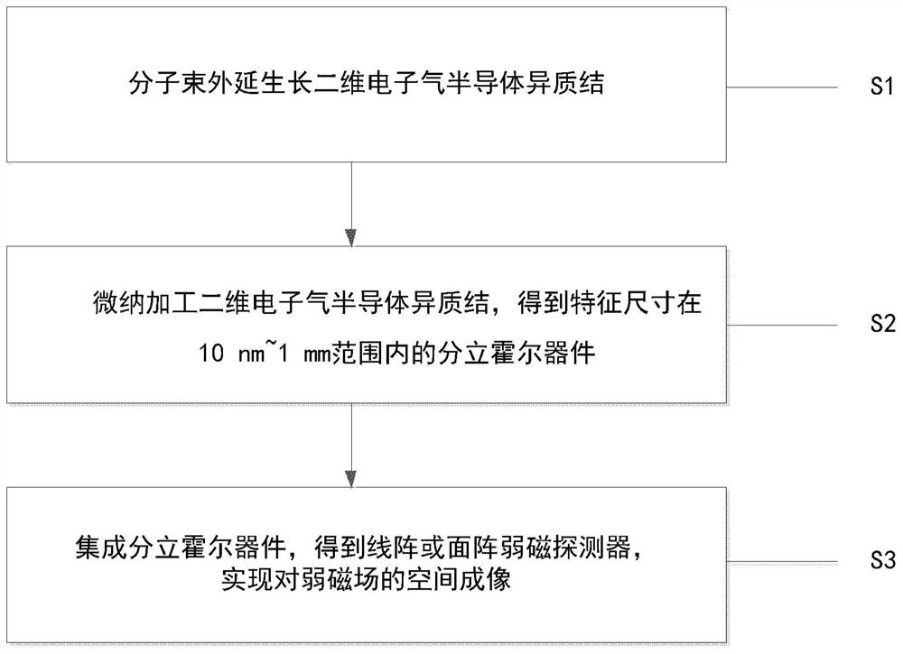
[0038] On the basis of the above examples, the preparation method of AlSb / InAs / AlSb semiconductor two-dimensional electron gas, please refer to figure 2 , including: S101, at a first temperature, molecular beam epitaxy grows a GaAs buffer layer on deoxidized semi-insulating GaAs (001); S102, lowers the first temperature to a second temperature, and sequentially molecular beam epitaxy AlSb buffer layer, (Al, Ga) Sb buffer layer; S103, reduce the second temperature to the third temperature, molecular beam epitaxy AlSb / InAs / AlSb semiconductor heterojunction on the (Al, Ga) Sb buffer layer; S104, in Molecular beam epitaxy of a layer of GaAs film on the surface of AlSb / InAs / AlSb semiconductor heterojunction is used to prevent its oxidation.
[0039] The purpose of growing the GaAs buffer layer by molecular beam epitaxy is to smooth the sample surface. The purpose of molecular beam epitaxy of AlSb buffer layer and (Al, Ga)Sb buffer layer is to gradually increase the lattice consta...
PUM
| Property | Measurement | Unit |
|---|---|---|
| thickness | aaaaa | aaaaa |
| thickness | aaaaa | aaaaa |
| thickness | aaaaa | aaaaa |
Abstract
Description
Claims
Application Information
 - R&D Engineer
- R&D Manager
- IP Professional
- Industry Leading Data Capabilities
- Powerful AI technology
- Patent DNA Extraction
Browse by: Latest US Patents, China's latest patents, Technical Efficacy Thesaurus, Application Domain, Technology Topic, Popular Technical Reports.
© 2024 PatSnap. All rights reserved.Legal|Privacy policy|Modern Slavery Act Transparency Statement|Sitemap|About US| Contact US: help@patsnap.com