Gain control circuit of ultrasonic flaw detector

A technology of gain control circuit and gain circuit, which is applied in the field of measurement, can solve the problems of insufficient intelligence, large signal waveform amplitude, single position for adjusting gain, etc., and achieve the effect of easy determination and good directionality

Pending Publication Date: 2020-12-08
青岛汉泰智能科技有限公司
View PDF0 Cites 0 Cited by
  • Summary
  • Abstract
  • Description
  • Claims
  • Application Information

AI Technical Summary

Problems solved by technology

[0002] When the signal received by the ultrasonic flaw detector is very weak, it is difficult for the ADC to accurately collect and convert the signal, so that the processor cannot accurately process the signal and display it on the display screen, making the amplitude of the signal waveform displayed on the display screen too large or too small , cannot be accurately displayed at about 60% of the display screen, so it is necessary to adjust the gain parameters of the signal, and adjust the gain in real time according to the strength of the signal, so that the signal can be accurately collected by the ADC and processed by the processor clearly displayed on the display;
[0003] Although the current ultrasonic flaw detector gain adjustment circuit can realize the adjustment of the gain, the position for adjusting the gain is single, and it cannot realize the real-time adjustment of different gradients in multiple places, which is not intelligent enough.
[0004] The existing technology can no longer meet the needs of people at the present stage. Based on the current situation, there is an urgent need to reform the existing technology

Method used


Image

  • Gain control circuit of ultrasonic flaw detector
  • Gain control circuit of ultrasonic flaw detector
  • Gain control circuit of ultrasonic flaw detector

Examples


Embodiment Construction

[0059] The following will clearly and completely describe the technical solutions in the embodiments of the present invention with reference to the accompanying drawings in the embodiments of the present invention. Obviously, the described embodiments are only some, not all, embodiments of the present invention. All other embodiments obtained by persons of ordinary skill in the art based on the present invention without making creative efforts fall within the protection scope of the present invention.

[0060] In the first aspect, the present invention provides an embodiment of a gain control circuit of an ultrasonic flaw detector, explaining the functions realized when the keys of the present invention work;

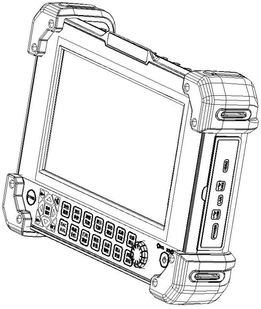
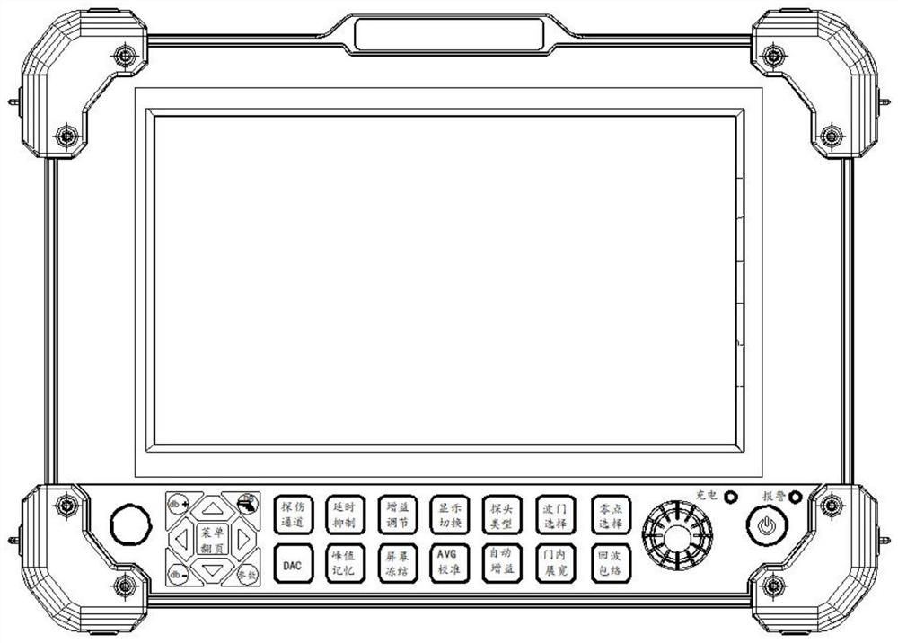
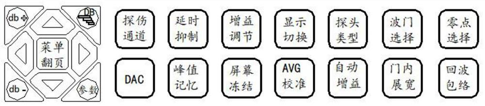
[0061] refer to Figure 1-3 , including a packaging shell, a display screen showing ultrasonic waveforms is provided in the middle of the front side of the packaging shell, and an operation panel is provided at the bottom of the display screen, and an area menu button i...


PUM


Abstract

The invention discloses a gain control circuit of an ultrasonic flaw detector. The circuit comprises a single-to-double gain circuit and a gain adjusting circuit, the single-to-double gain circuit isprovided with a gain amplifier with a fixed 6db, and the positive input terminal of the gain amplifier is electrically connected with the output terminal of an ultrasonic receiving loop through an LCfilter circuit consisting of an inductor L5 and a blocking capacitor C23; the gain adjusting circuit comprises a DAC for converting analog signals, and a D-end control pin of the DAC is electrically connected with an FPGA. And the DAC converts a digital signal of the FPGA into an analog signal for controlling the VGA through the D-end control pin. Gain adjustment is further performed on the VGA1 and the VGA2 through the analog signal, and the gain amplifier converts an ultrasonic receiving loop reflection signal at the input terminal into a differential gain signal and outputs the differentialgain signal to the VGA1, so that the noise of the ultrasonic reflection signal is effectively reduced; and the repetition frequency of the negative pulse in the ultrasonic transmitting circuit is suppressed.

Description

technical field [0001] The invention relates to the technical field of measurement, in particular to a gain control circuit of an ultrasonic flaw detector. Background technique [0002] When the signal received by the ultrasonic flaw detector is very weak, it is difficult for the ADC to accurately collect and convert the signal, so that the processor cannot accurately process the signal and display it on the display screen, making the amplitude of the signal waveform displayed on the display screen too large or too small , cannot be accurately displayed at about 60% of the display screen, so it is necessary to adjust the gain parameters of the signal, and adjust the gain in real time according to the strength of the signal, so that the signal can be accurately collected by the ADC and processed by the processor clearly displayed on the display; [0003] Although the current ultrasonic flaw detector gain adjustment circuit can realize the adjustment of the gain, the position...

Claims


Application Information

Patent Timeline
Patent Type & Authority Applications(China)
IPC IPC(8): G01N29/44
CPCG01N29/4463
Inventor 郝春华
Owner 青岛汉泰智能科技有限公司
Why Eureka
Try Eureka