Error amplifier circuit with switched capacitor compensation

An error amplifier, switched capacitor technology, applied in amplifiers, improved amplifiers to reduce temperature/power supply voltage changes, high-efficiency power electronic conversion, etc., can solve the problems of increasing chip pins, inability to integrate, increasing system area and cost, etc. The effect of avoiding pins, wide application and reducing system area

Active Publication Date: 2020-11-27
UNIV OF ELECTRONICS SCI & TECH OF CHINA
View PDF3 Cites 0 Cited by
  • Summary
  • Abstract
  • Description
  • Claims
  • Application Information

AI Technical Summary

Problems solved by technology

C CC Usually nF to uF level is required, which cannot be integrated into the system, but can only be plugged in, which not only increases the chip pins, but also increases the system area and cost

Method used


Image

  • Error amplifier circuit with switched capacitor compensation
  • Error amplifier circuit with switched capacitor compensation
  • Error amplifier circuit with switched capacitor compensation

Examples


Embodiment Construction

[0026] The present invention will be further elaborated below in conjunction with the accompanying drawings and specific embodiments.

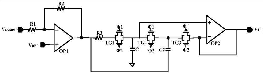
[0027] like figure 2 Shown is a structural schematic diagram of an error amplifier circuit with switched capacitor compensation proposed by the present invention, wherein the first operational amplifier OP1 is the main circuit of the error amplifier, and the first resistor R1 and the second resistor R2 are used to determine the low-frequency gain of the loop , the third resistor R3, the first transmission gate TG1, the second transmission gate TG2, the third transmission gate TG3, the first capacitor C1 and the second capacitor C2 are components of the switched capacitor compensation scheme, and the second operational amplifier OP2 is used as a buffer The BUFFER circuit (BUFFER) prevents subsequent circuits from drawing current from here, affecting loop compensation. The first operational amplifier OP1 and the second operational amplifier OP...


PUM


Abstract

An error amplifier circuit with switched capacitor compensation is characterized in that: a positive input end of a first operational amplifier is connected with a reference voltage, a negative inputend is connected with one end of a second resistor and connected with an application system for output sampling through a first resistor, and an output end is connected with the other end of the second resistor, one end of a third resistor and one end of a second capacitor; one end of a first transmission gate is connected with the other end of the third resistor, and the other end is connected with one end of a second transmission gate and a positive input end of a second operational amplifier and then grounded through a first capacitor; and one end of a third transmission gate is connected with the other end of the second transmission gate and the other end of the second capacitor, and the other end is connected with a negative input end and an output end of the second operational amplifier. According to the error amplifier circuit, the three transmission gates are controlled to be conducted and cut off by combining a clock, so that the capacitance and the resistance of the access system are changed to realize an equivalent capacitance amplification effect, the phase margin of the system is ensured to be stable enough under an internal integrated compensation scheme with small capacitance, and the reliability and the area cost are both considered.

Description

technical field [0001] The invention belongs to the technical field of analog integrated circuits, and relates to an error amplifier circuit with switch capacitance compensation, which can be applied to a DC-DC converter to realize loop stability. Background technique [0002] In recent years, the continuous development of modern power electronics technology has promoted the vigorous development of industrial control instruments, automotive electronics, and personal consumer electronics markets, and the rapidly growing Internet of Things and increasingly complex electronic systems such as portable devices are the market demand for power management ICs. Bringing strong impetus and strict requirements. The most common type of power management IC is the DC-DC converter of switching power supply. Due to its advantages of high power efficiency, fast response speed, large input and output voltage range, and high output current, etc. In practical applications, it is suitable for m...

Claims


Application Information

Patent Timeline
Patent Type & Authority Applications(China)
IPC IPC(8): H03F1/30H02M3/00
CPCH03F1/303H02M3/00H02M1/0016H02M1/0003Y02B70/10
Inventor 周泽坤肖志平许王帅王卓张波
Owner UNIV OF ELECTRONICS SCI & TECH OF CHINA
Why Eureka
Try Eureka