LED light-emitting part manufacturing method, LED light-emitting part and light-emitting device

A manufacturing method and technology for light-emitting parts, which can be applied to printing devices, electrical components, and electrical solid-state devices, etc., can solve the problems of easily damaged circuit boards, limited application, and low yield of miniLED finished products.

Inactive Publication Date: 2020-11-10
SHENZHEN JUFEI OPTOELECTRONICS
View PDF8 Cites 0 Cited by
  • Summary
  • Abstract
  • Description
  • Claims
  • Application Information

AI Technical Summary

Problems solved by technology

[0003] The technical problem to be solved by the present invention is that the existing mini LED manufacturing process is easy to damage the circuit board, resulting in a low

Method used


Image

  • LED light-emitting part manufacturing method, LED light-emitting part and light-emitting device
  • LED light-emitting part manufacturing method, LED light-emitting part and light-emitting device
  • LED light-emitting part manufacturing method, LED light-emitting part and light-emitting device

Examples


no. 1 example

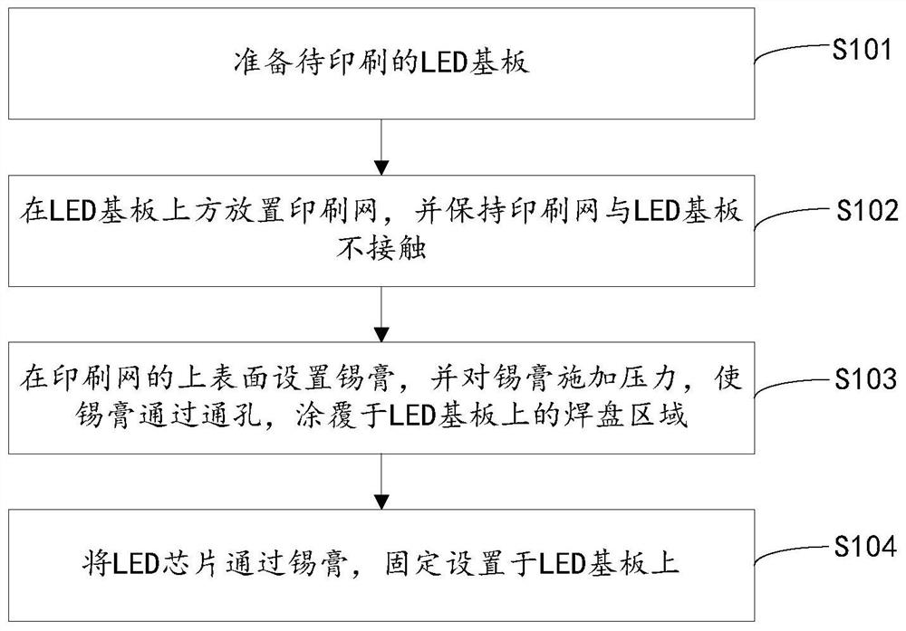
[0028] This embodiment provides an LED lighting device manufacturing method, refer to Figure 1-3 This method includes:

[0029] S101, ready LED substrate 1 to be printed;

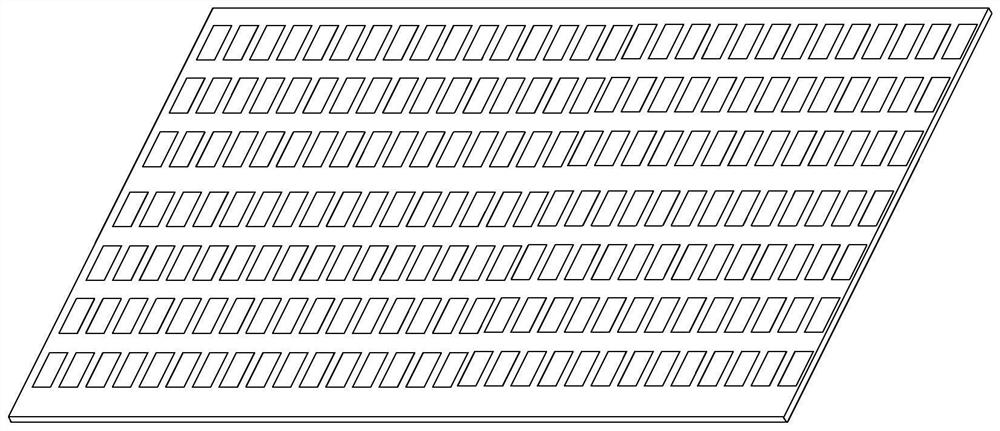
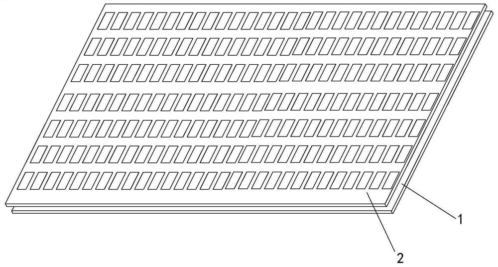
[0030] S102, the substrate 1 is placed above the LED printing network 2, and holds the printed web 21 is not in contact with the LED substrate; printing on the web 2 with a through hole on a pad region corresponding to the LED board;

[0031] S103, solder paste is provided on a surface of the printing screen 2, and pressure is applied paste, the paste through the through hole so that, applied to the pad region on the substrate 1 LED;

[0032] S104, the LED chip 11 through the solder paste, and fixed to the LED board 1.

[0033] In this embodiment, LED light emitting element refers to the Mini LED light emitting element, the basic structure is provided in a plurality of the LED chip 11 on the substrate 1, wherein the LED chip 11 according to certain rules are arranged to form an array, the number of LED chips 11...

no. 2 example

[0056] This embodiment provides an LED lighting device manufacturing method, please continue to refer to figure 1 This method includes:

[0057] S101, ready LED substrate 1 to be printed;

[0058] S102, the substrate 1 is placed above the LED printing network 2, and holds the printed web 21 is not in contact with the LED substrate; printing on the web 2 with a through hole on a pad region corresponding to the LED board;

[0059] S103, solder paste is provided on a surface of the printing web 2, by a doctor blade and the paste through the through hole, applied to the pad region on the substrate 1 LED;

[0060] S104, the LED chip 11 through the solder paste, and fixed to the LED board 1.

[0061] Wherein, in the embodiment, the through holes 2 on the printing screen is small is large in the present embodiment, the through-hole portion close to the size of an LED substrate 1 is larger than size of the LED away from the portion of the substrate 1. In the present embodiment the printin...


PUM

PropertyMeasurementUnit
Heightaaaaaaaaaa

Abstract

The invention provides an LED light-emitting part manufacturing method, an LED light-emitting part and a light-emitting device. The LED light-emitting part manufacturing method comprises the steps: preparing an LED substrate to be printed; placing a printing screen above the LED substrate, and keeping the printing screen not in contact with the LED substrate; forming through holes corresponding tothe bonding pad areas on the LED substrate in the printing net; arranging solder paste on the upper surface of the printing net, and applying pressure to the solder paste, so the solder paste passesthrough the through holes and coats the bonding pad area on the LED substrate; and fixedly arranging the LED chip on the LED substrate through solder paste. Therefore, during manufacturing, the LED substrate is not in contact with the printing net, so when the scraper is used, solder paste can smoothly flow down through the through holes, the printing net can be prevented from being in contact with the LED substrate to damage a circuit layer of the LED substrate, and the manufacturing yield of the LED light-emitting part is increased.

Description

Technical field [0001] The present invention relates to a light emitting diode (LED), and more particularly, to a method for manufacturing the LED light emitting element, the LED light emitting element and the light emitting device. Background technique [0002] With social progress and development, technological innovation is also a display device, which came into mini LED. Mini for LED applications, because of its small particle LED chip, die bonding step which usually flip printing process, each LED circuit board Mini typically have thousands of solder joints, welds or even millions to connect the RGB three-color chips. Such a huge amount of solder, to the chip package is a big difficulty, since the ultra-dense small space requirements, the use of LED Mini LED chip size of m level, and the line thickness of the LED substrate surface is usually very thin, only 2 -5um, conventional printing surface of the substrate against the printing screen printing, doctor blade pressure, pre...

Claims


Application Information

Patent Timeline
IPC IPC(8): H01L33/62H01L33/48H01L33/54H01L25/075B41M3/00B41M1/12B41F15/36
CPCB41F15/36B41M1/12B41M3/003H01L25/0753H01L33/48H01L33/54H01L33/62H01L2933/0033H01L2933/0041H01L2933/005
Inventor 曹金涛孙平如陈彦铭刘永邢美正
Owner SHENZHEN JUFEI OPTOELECTRONICS
Why Eureka
Try Eureka