Flexible large-area perovskite photovoltaic device and preparation method thereof
A photovoltaic device and perovskite technology, which is applied in semiconductor/solid-state device manufacturing, photovoltaic power generation, electric solid-state devices, etc., can solve the problems of small crystal particle size and poor crystallinity of perovskite film, and achieve the removal of internal stress and improve Mechanical flexibility, performance-enhancing effect
- Summary
- Abstract
- Description
- Claims
- Application Information
AI Technical Summary
Problems solved by technology
Method used
Image

Examples
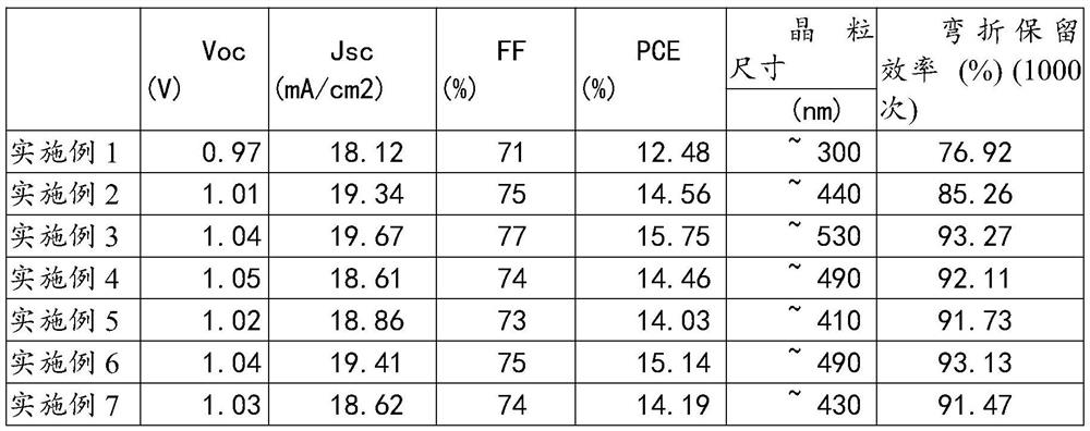
Embodiment 1
[0036] Embodiment 1 (control group):
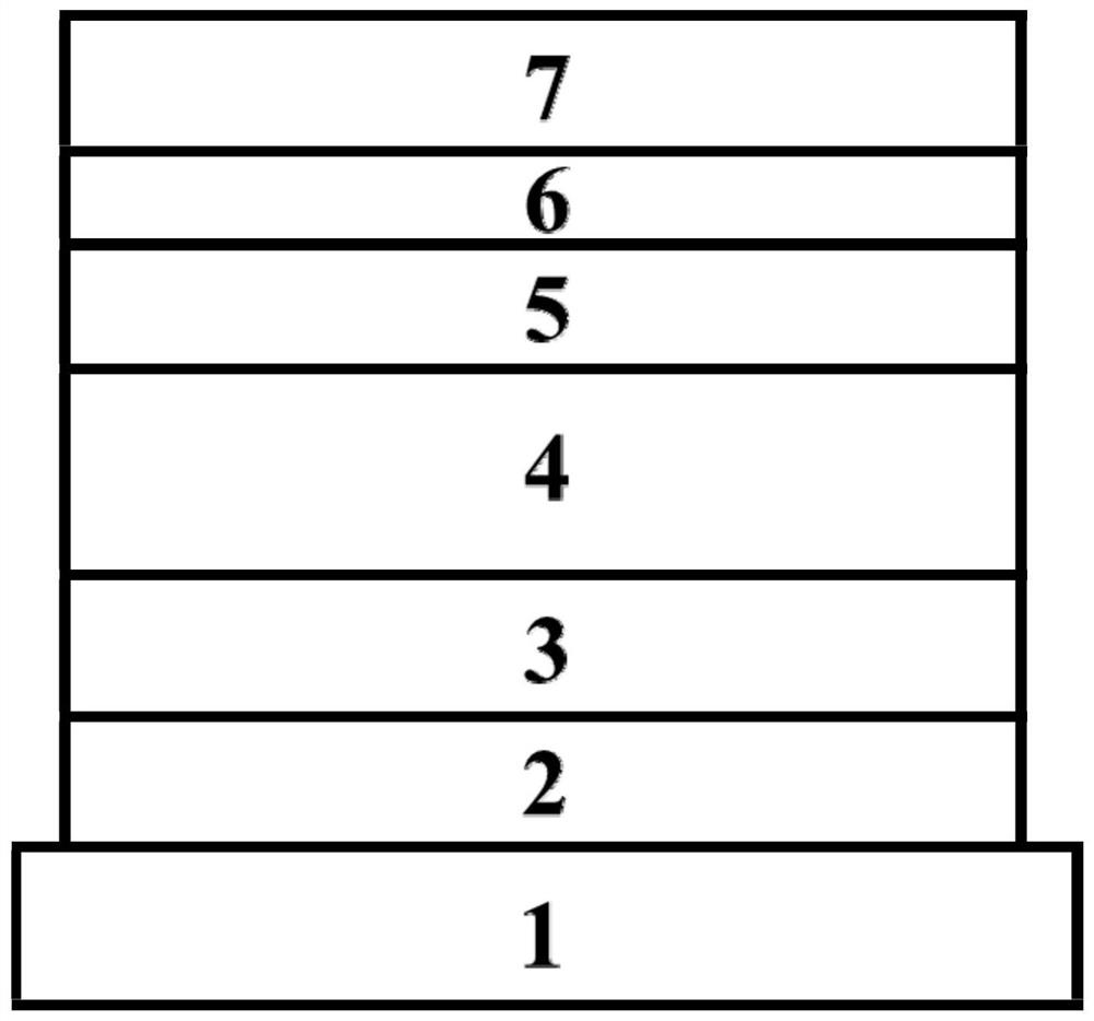
[0037] 1. Clean the substrate composed of flexible PI substrate 1 and transparent conductive anode ITO layer 2 with surface roughness less than 1nm, and dry it with nitrogen after cleaning;
[0038]2. Spin-coat PEDOT:PSS (3000rpm, 60s, 45nm) on the surface of the transparent conductive anode ITO layer 2 to prepare the PEDOT:PSS anode buffer layer 3, and thermally anneal the formed film (150°C, 1h);
[0039] 3. Drop-coat the MAPbI3 (20mg / ml) perovskite solution on the edge of the PEDOT:PSS anode buffer layer 3, and prepare the solid-state perovskite active layer 4 by spin coating, and add chlorine dropwise during the remaining 25s of spin coating Benzene anti-solvent (200ul), and thermal annealing (100°C, 10min);
[0040] 4. Spin-coat the PCBM electronic buffer layer 5 on the perovskite active layer 4, and perform thermal annealing (120°C, 10min);
[0041] 5. Under the condition of vacuum degree of 3*10-3Pa, Bphen (10nm) was evaporated o...
Embodiment 2
[0046] 1. Clean the substrate composed of flexible PI substrate 1 and transparent conductive anode ITO layer 2 with surface roughness less than 1nm, and dry it with nitrogen after cleaning;
[0047] 2. Spin-coat PEDOT:PSS (3000rpm, 60s, 45nm) on the surface of the transparent conductive anode ITO layer 2 to prepare the PEDOT:PSS anode buffer layer 3, and thermally anneal the formed film (150°C, 1h);
[0048] 3. Drop-coat the MAPbI3 (20mg / ml) perovskite solution on the edge of the PEDOT:PSS anode buffer layer 3, and prepare the solid-state perovskite active layer 4 by spin coating, and add chlorine dropwise during the remaining 25s of spin coating Benzene anti-solvent (200ul);
[0049] 4. Place the obtained perovskite active layer 4 in a low temperature environment (0°C, 30min), and then quickly transfer the film to a constant temperature platform for rapid thermal annealing (100°C, 10min);
[0050] 5. Spin-coat the PCBM electronic buffer layer 5 on the perovskite active layer...
Embodiment 3
[0056] 1. Clean the substrate composed of flexible PI substrate 1 and transparent conductive anode ITO layer 2 with surface roughness less than 1nm, and dry it with nitrogen after cleaning;
[0057] 2. Spin-coat PEDOT:PSS (3000rpm, 60s, 45nm) on the surface of the transparent conductive anode ITO layer 2 to prepare the PEDOT:PSS anode buffer layer 3, and thermally anneal the formed film (150°C, 1h);
[0058] 3. Drop-coat the MAPbI3 (20mg / ml) perovskite solution on the edge of the PEDOT:PSS anode buffer layer 3, and prepare the solid-state perovskite active layer 4 by spin coating, and add chlorine dropwise during the remaining 25s of spin coating Benzene anti-solvent (200ul);
[0059] 4. Place the obtained perovskite active layer 4 in a low temperature environment (-10°C, 30min), and then quickly transfer the film to a constant temperature platform for rapid thermal annealing (100°C, 10min);
[0060] 5. Spin-coat the PCBM electronic buffer layer 5 on the perovskite active lay...
PUM
| Property | Measurement | Unit |
|---|---|---|
| area | aaaaa | aaaaa |
| thickness | aaaaa | aaaaa |
| thermal resistance | aaaaa | aaaaa |
Abstract
Description
Claims
Application Information
 - R&D
- Intellectual Property
- Life Sciences
- Materials
- Tech Scout
- Unparalleled Data Quality
- Higher Quality Content
- 60% Fewer Hallucinations
Browse by: Latest US Patents, China's latest patents, Technical Efficacy Thesaurus, Application Domain, Technology Topic, Popular Technical Reports.
© 2025 PatSnap. All rights reserved.Legal|Privacy policy|Modern Slavery Act Transparency Statement|Sitemap|About US| Contact US: help@patsnap.com