Semiconductor packaging method and semiconductor packaging structure
A packaging method and packaging structure technology, applied in the direction of semiconductor devices, semiconductor/solid-state device manufacturing, semiconductor/solid-state device components, etc., can solve the problems of edge pins and solder falling off, cracking, etc., to improve the bonding force and strength. , the effect of improving reliability
- Summary
- Abstract
- Description
- Claims
- Application Information
AI Technical Summary
Problems solved by technology
Method used
Image
Examples
Embodiment 1
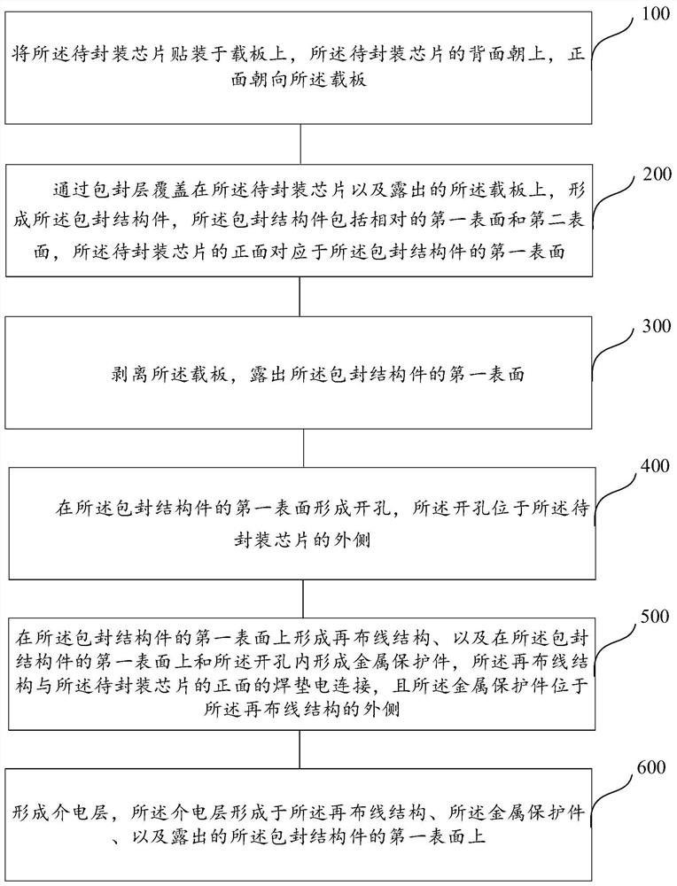
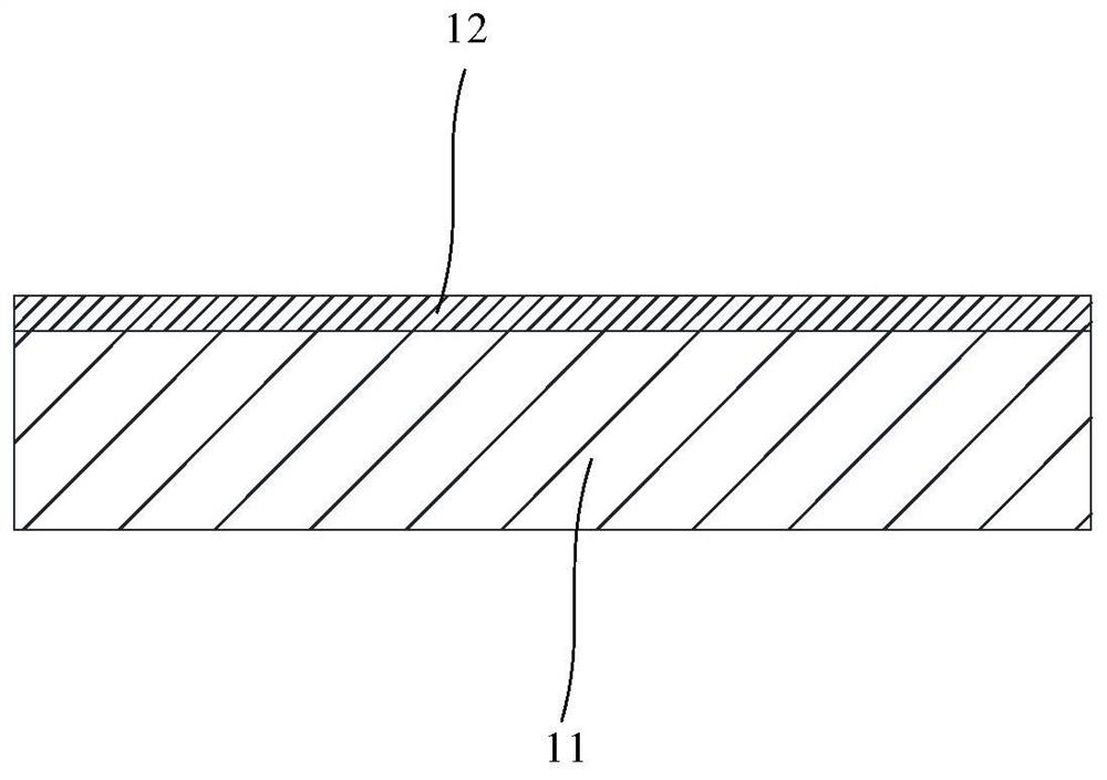
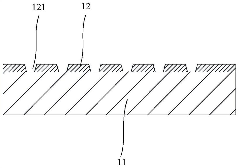
[0042] Such as figure 1 , Figure 2(a)-Figure 2(m) as well as image 3 As shown, the present application provides a semiconductor packaging method and a semiconductor packaging structure.
[0043] figure 1 It is a flowchart of a semiconductor packaging method proposed according to an exemplary embodiment of the present application. Such as figure 1 As shown, the semiconductor packaging method includes the following steps:
[0044] Step 100: Mount the chip to be packaged on a carrier board, with the back side of the chip to be packaged facing up and the front side facing the carrier board;
[0045]Step 200: Covering the chip to be packaged and the exposed carrier with an encapsulation layer to form the encapsulation structure, the encapsulation structure includes opposite first surfaces and second surfaces, the The front side of the chip to be packaged corresponds to the first surface of the encapsulation structure;
[0046] Step 300: Peel off the carrier board to expose...
Embodiment 2
[0114] The content of the semiconductor packaging method in this embodiment is basically the same as that of the semiconductor packaging method in Embodiment 1, the difference is that in step 400, the depth of the opening is equal to the thickness of the encapsulation structure, That is, the opening penetrates the encapsulation structure along the thickness direction, so it is difficult to fill the entire opening through a single electroplating process, but after step 400 and before step 500, the semiconductor packaging method further includes:
[0115] Step 450: forming a metal layer on the inner surface of the opening, which may firstly fill a part of the space in the opening 15 .
[0116] In step 400, as shown in FIG. 4(a), the depth d1 of the opening 15 formed on the second surface 10b of the encapsulating structural member 10 is equal to the thickness t1 of the encapsulating structural member 10, that is, the opening 15 along the thickness The direction T runs through the...
Embodiment 3
[0126] The content of the semiconductor packaging method in this embodiment is basically the same as the semiconductor packaging method in Embodiment 2, the difference is that after step 600, that is, after the formation of the dielectric layer, it also includes: A heat dissipation fin is formed on the second surface of the encapsulation structure, and the heat dissipation fin is connected to the metal protection element exposed on the second surface of the encapsulation structure. Since the depth of the opening is equal to the thickness of the encapsulating structure, that is, the opening penetrates the enclosing structure along the thickness direction, the metal protection formed therein will be exposed on the second side of the enclosing structure. surface.
[0127] Specifically, as shown in FIG. 6(a), a heat dissipation fin 60 is formed on the second surface 10b of the encapsulation structure 10, and the heat dissipation fin 60 and the metal protection member 50 are expose...
PUM
 Abstract
Description
Claims
Application Information
 - Generate Ideas
- Intellectual Property
- Life Sciences
- Materials
- Tech Scout
- Unparalleled Data Quality
- Higher Quality Content
- 60% Fewer Hallucinations
Browse by: Latest US Patents, China's latest patents, Technical Efficacy Thesaurus, Application Domain, Technology Topic, Popular Technical Reports.
© 2025 PatSnap. All rights reserved.Legal|Privacy policy|Modern Slavery Act Transparency Statement|Sitemap|About US| Contact US: help@patsnap.com


