Vertical integrated unit diode chip
A technology of integrating cells and diodes, applied in electrical components, electro-solid devices, circuits, etc., to solve problems such as LED light efficiency, heat dissipation and stability limitations
- Summary
- Abstract
- Description
- Claims
- Application Information
AI Technical Summary
Problems solved by technology
Method used
Image

Examples
Embodiment 1
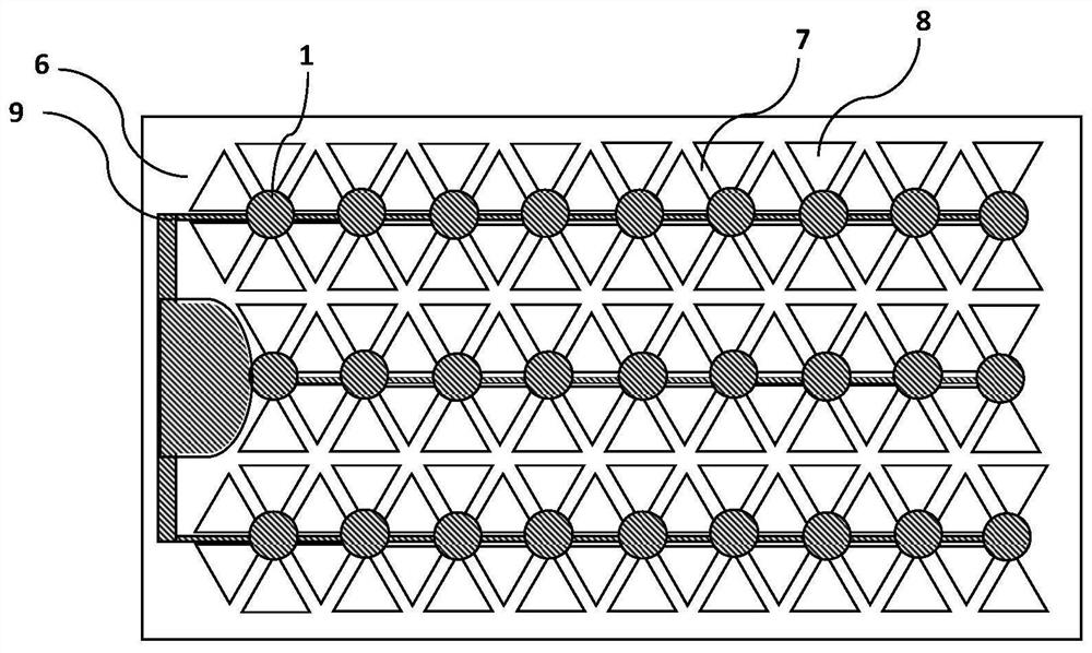
[0055] This embodiment provides a vertically integrated unit diode chip, including: a second conductivity type electrode 1 , a diode mesa structure 6 , a trench 7 , a diode unit 8 and an electrode line 9 .
[0056] like image 3 As shown, the diode mesa structure includes 6 rows of 102 equally sized and uniformly distributed triangular diode units, and the length of the diode units along the x-axis direction is 40 microns. The diode mesa structure adopts a triangular arrangement, and the size of the mesa structure is smaller than the current diffusion length. The diode units are triangular in shape and distributed according to a uniform symmetrical arrangement. The electrode wire is an electrode connecting wire between diode units, the width of the electrode wire is 0.001-20 microns, and the thickness is 0.001-10 microns.
[0057] like Figure 4 As shown, the diode mesa structure includes 6 rows of 6 rectangular diode units with uniform sizes, and the length of the diode un...
Embodiment 2
[0062] This embodiment provides a vertically mounted integrated unit diode chip, comprising a first conductivity type layer 5, a second conductivity type layer 3, a quantum well active region 4 on the first conductivity type layer, and a second conductivity type electrode 1. The insulating medium layer 2, wherein the layer of the first conductivity type is a p-GaN layer, the layer of the second conductivity type is an n-GaN layer, and the electrode of the second conductivity type is an n-electrode. The trench structure is located between the diode units, and the trench depth is L. The thickness of the n-GaN layer is L2, the thickness of the quantum well active region is L3, and the thickness of the p-GaN layer is L1.
[0063] like Image 6 As shown, etching from the n-GaN layer to the p-GaN layer to half the thickness of the p-GaN layer, the relationship between the trench depth L and L1, L2 and L3 is: L=L1+L3+0.5*L2.
[0064] like Figure 7 As shown, when etching from the ...
Embodiment 3
[0066] This embodiment provides a vertically mounted integrated unit diode chip, such as Figure 8 As shown, the diode mesa structure includes 4 rows of a total of 30 ladder-shaped diode units of equal size and uniform distribution, and the length of the diode unit along the x-axis direction is 40 microns. The size of the mesa structure is smaller than the diffusion length of the current injection. The shape of the diode units is trapezoidal and distributed according to a uniform symmetrical arrangement. The angle between the side wall of the diode unit and the horizontal plane is greater than 0 degrees and less than or equal to 90 degrees, and the shape of the side wall of the diode unit is trapezoidal.
[0067] like Figure 9 As shown, the diode cell has a sidewall surface with grooves distributed from the bottom to the top of the mesa. The cross-sectional shape of the trench on the side wall of the diode unit is triangular, the width of the trench on the side wall is 0.5...
PUM
| Property | Measurement | Unit |
|---|---|---|
| Width | aaaaa | aaaaa |
| Thickness | aaaaa | aaaaa |
| Diameter | aaaaa | aaaaa |
Abstract
Description
Claims
Application Information
 - R&D
- Intellectual Property
- Life Sciences
- Materials
- Tech Scout
- Unparalleled Data Quality
- Higher Quality Content
- 60% Fewer Hallucinations
Browse by: Latest US Patents, China's latest patents, Technical Efficacy Thesaurus, Application Domain, Technology Topic, Popular Technical Reports.
© 2025 PatSnap. All rights reserved.Legal|Privacy policy|Modern Slavery Act Transparency Statement|Sitemap|About US| Contact US: help@patsnap.com