
Positioning method and positioning device for target position of semiconductor chip sample

A technology of target position and positioning method, which is applied in semiconductor/solid-state device manufacturing, electrical components, circuits, etc., and can solve problems such as the inability to observe the structure of the device area, the inability to ensure the integrity of the target position, and the transmission depth of the scanning electron microscope for grinding inhomogeneity.

Active Publication Date: 2020-10-27
YANGTZE MEMORY TECH CO LTD
View PDF4 Cites 1 Cited by
  • Summary
  • Abstract
  • Description
  • Claims
  • Application Information

AI Technical Summary

Problems solved by technology

[0002] In the development of semiconductor technology, with the improvement of technology and process technology, how to efficiently and accurately find the target position and ensure the integrity of the target position has become one of the many difficult challenges. For all semiconductor chips, the entire The device area usually has a large area. With the traditional method of observing with a scanning electron microscope after grinding, it is impossible to observe the structure of the entire device area and determine the target due to the problems of scanning range, grinding inhomogeneity and scanning electron microscope transmission depth. position or needs to be repeatedly polished many times to observe the device area completely and then determine the target position, so there is a great risk of over-grinding the target position, the integrity of the target position cannot be guaranteed, and repeated grinding confirmation of the sample is also very consuming time

Method used


Image

  • Positioning method and positioning device for target position of semiconductor chip sample
  • Positioning method and positioning device for target position of semiconductor chip sample
  • Positioning method and positioning device for target position of semiconductor chip sample

Examples


Embodiment Construction

[0027] A method for locating a target position of a semiconductor chip sample and a device 1000 for locating a target position of a semiconductor chip sample proposed by the present invention will be further described in detail below with reference to the accompanying drawings and specific embodiments.

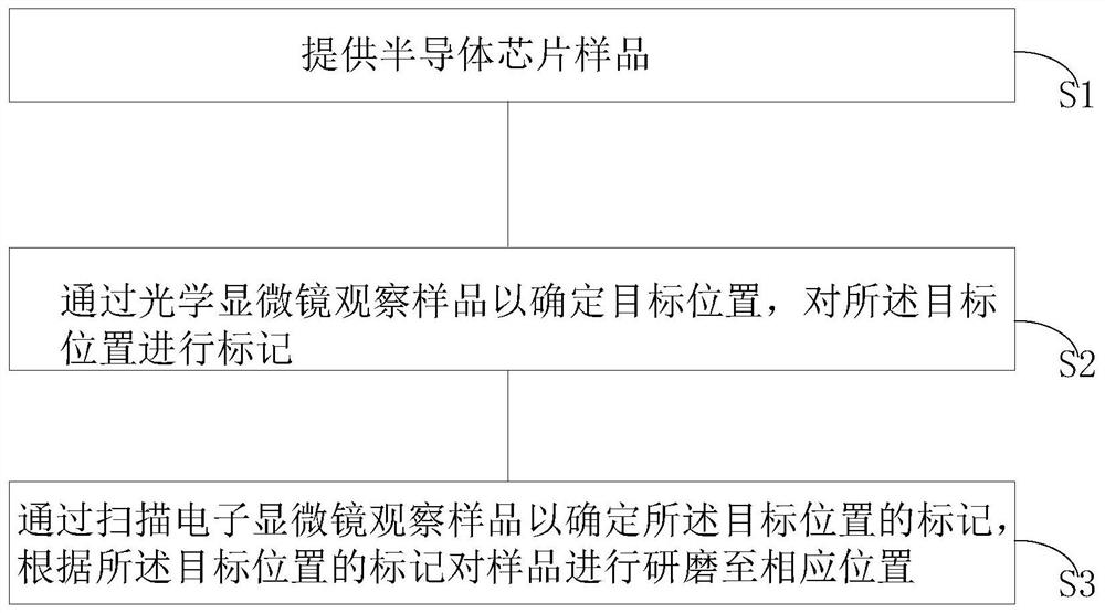
[0028] The method for locating the target position of a semiconductor chip sample according to an embodiment of the present invention will be described below with reference to the accompanying drawings. figure 1 and Figure 3-Figure 5 As shown, the positioning method of the semiconductor chip sample target position according to the embodiment of the present invention includes the following steps:

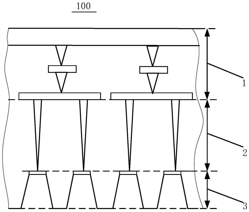
[0029] S1: provide a semiconductor chip sample 100; for the semiconductor chip sample 100, if image 3 As shown, the semiconductor chip sample 100 may include an interlayer dielectric layer 2 and a device region layer 3, the interlayer dielectric layer 2 is located above the device...


PUM


Abstract

The invention discloses a positioning method and a positioning device for a target position of a semiconductor chip sample. The positioning method comprises the following steps: S1, providing the semiconductor chip sample; S2, observing the sample through an optical microscope to determine a target position, and marking the target position; and S3, observing the sample through an electron microscope to determine the mark of the target position, and grinding the sample to the corresponding position according to the mark of the target position. According to the method for positioning the targetposition of the semiconductor chip sample, the sample can be processed after the target position is determined, so that excessive grinding can be avoided, the integrity of the target position can be ensured, and the scanning range and the sample preparation time can be reduced.

Description

technical field [0001] The invention relates to the technical field of semiconductors, in particular to a positioning method and a positioning device for a target position of a semiconductor chip sample. Background technique [0002] In the development of semiconductor technology, with the improvement of technology and process technology, how to efficiently and accurately find the target position and ensure the integrity of the target position has become one of the many difficult challenges. For all semiconductor chips, the entire The device area usually has a large area. With the traditional method of observing with a scanning electron microscope after grinding, it is impossible to observe the structure of the entire device area and determine the target due to the problems of scanning range, grinding inhomogeneity and scanning electron microscope transmission depth. position or needs to be repeatedly polished many times to observe the device area completely and then determi...

Claims


Application Information

Patent Timeline
Patent Type & Authority Applications(China)
IPC IPC(8): H01L21/68H01L21/67H01L21/3105H01L21/311
CPCH01L21/31053H01L21/31111H01L21/67092H01L21/67282H01L21/68H01L21/681
Inventor 邹锭
Owner YANGTZE MEMORY TECH CO LTD
Learn More