Film bulk acoustic resonator and manufacturing process thereof
A thin-film bulk acoustic wave and manufacturing process technology, applied in electrical components, impedance networks, etc., can solve problems such as taking away energy, affecting device performance, and difficult to suppress parasitic oscillations
- Summary
- Abstract
- Description
- Claims
- Application Information
AI Technical Summary
Problems solved by technology
Method used
Image
Examples
Embodiment Construction
[0038] The application will be further described in detail below with reference to the drawings and embodiments. It can be understood that the specific embodiments described here are only used to explain the related invention, but not to limit the invention. In addition, it should be noted that, for ease of description, only the parts related to the relevant invention are shown in the drawings.
[0039] It should be noted that the embodiments in the application and the features in the embodiments can be combined with each other if there is no conflict. Hereinafter, the present application will be described in detail with reference to the drawings and in conjunction with embodiments.
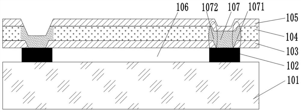
[0040] figure 1 Shows a cross-sectional view of a thin film bulk acoustic resonator according to an embodiment of the present invention, such as figure 1 As shown, the thin film bulk acoustic wave resonator includes a substrate 101, a support layer 102, a bottom electrode 103, a piezoelectric layer 1...
PUM
 Abstract
Description
Claims
Application Information
 - R&D Engineer
- R&D Manager
- IP Professional
- Industry Leading Data Capabilities
- Powerful AI technology
- Patent DNA Extraction
Browse by: Latest US Patents, China's latest patents, Technical Efficacy Thesaurus, Application Domain, Technology Topic, Popular Technical Reports.
© 2024 PatSnap. All rights reserved.Legal|Privacy policy|Modern Slavery Act Transparency Statement|Sitemap|About US| Contact US: help@patsnap.com


