Chip transfer processing device and method

A processing device and chip transfer technology, applied in transportation and packaging, electrical components, semiconductor/solid-state device manufacturing, etc., can solve the problems of low processing efficiency of traditional devices

Pending Publication Date: 2020-10-23
深圳市诺泰芯装备有限公司
View PDF0 Cites 2 Cited by
  • Summary
  • Abstract
  • Description
  • Claims
  • Application Information

AI Technical Summary

Problems solved by technology

[0006] Aiming at the deficiencies of the prior art, the present invention provides a chip transfer processing device and method, which has the advantages of improving processing efficiency, and solves the problem of low processing efficiency of the traditional device mentioned in the above-mentioned background technology

Method used


Image

  • Chip transfer processing device and method
  • Chip transfer processing device and method
  • Chip transfer processing device and method

Examples


Embodiment Construction

[0041] The following will clearly and completely describe the technical solutions in the embodiments of the present invention with reference to the accompanying drawings in the embodiments of the present invention. Obviously, the described embodiments are only some, not all, embodiments of the present invention. Based on the embodiments of the present invention, all other embodiments obtained by persons of ordinary skill in the art without making creative efforts belong to the protection scope of the present invention.

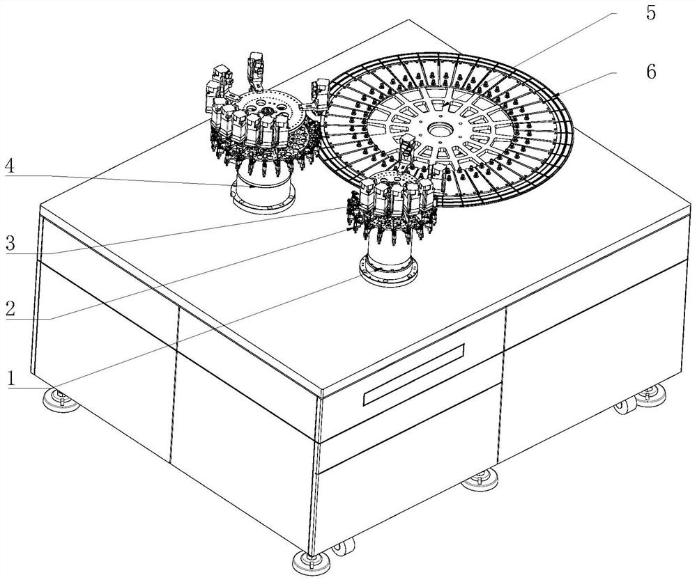
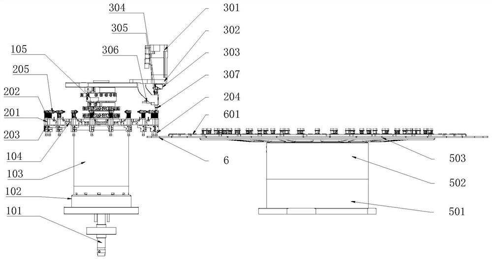
[0042] see Figure 1-6 , a chip transfer processing device and method, including a first turret module 1 , a second turret module 4 and a carrier turret module 5 .

[0043] The first turret module 1 includes a vacuum air guide rod 101, and the vacuum air guide rod 101 is used to provide vacuum negative pressure to the device vacuum suction nozzle 204, so that the device vacuum suction nozzle 204 can absorb components, and the vacuum air guide rod 101 The oute...


PUM


Abstract

The invention relates to the technical field of semiconductor processing and further discloses a chip transfer processing device and method. The device comprises a first turret module, a second turretmodule and a tray turret module, wherein a suction nozzle support mechanism is arranged on an outer surface of the first turret module, a linear pressing mechanism is arranged at an upper end of thefirst turret module, the second turret module is arranged on the side surface of the first turret module, a carrying tray turret module is arranged on the side surface of the first turret module, anda device carrying tray device is arranged at the top of the carrying tray turret module. The chip transfer processing device is advantaged in that the first turret module and the second turret moduleare arranged on a cabinet, and meanwhile, a tray turret module is arranged, positioning is conducted through a position detection sensor, expansion and compatibility of production processes such as processing, visual inspection, electrical property testing, laser printing, product classification and finished product packaging in the rear-section production and manufacturing process of electronic chip products are facilitated, manpower is saved, and production efficiency is improved.

Description

technical field [0001] The invention relates to the technical field of semiconductor processing, in particular to a chip transfer processing device and method. Background technique [0002] In the post-production process of electronic chip products, it is necessary for the electronic chip to be transferred in a high-speed, accurate and reliable spatial position, so as to realize efficient processing of electronic chip products, visual inspection, electrical testing, laser printing, Product classification, finished product packaging and other production process requirements. [0003] The traditional method is to use a vacuum nozzle to pick up the chip and transfer it to the spatial position, so as to carry out the processing of electronic chip products, visual inspection, electrical testing, laser printing, product classification, finished product packaging and other production processes. Due to the many processes and limited number of suction nozzles in the back-end manufac...

Claims


Application Information

Patent Timeline
IPC IPC(8): H01L21/677
CPCH01L21/67706H01L21/67721H01L21/67736
Inventor 李辉王体李俊强
Owner 深圳市诺泰芯装备有限公司
Why Eureka
Try Eureka