Solid-state imaging element and electronic apparatus
A solid-state imaging and component technology, applied in optical components, electrical components, electric solid devices, etc., can solve problems such as color mixing and phenomena, and achieve the effects of easy processing, high degree of freedom, and improved image quality
Inactive Publication Date: 2013-10-23
SONY SEMICON SOLUTIONS CORP
View PDF6 Cites 0 Cited by
- Summary
- Abstract
- Description
- Claims
- Application Information
AI Technical Summary
Problems solved by technology
As a result, this is prone to problems such as smearing and color mixing
Method used
View moreImage
Smart ImageViewing Examples


Examples
no. 1 example
[0041] 1. First Embodiment (Solid State Imaging Element)
no. 2 example
[0042] 2. Second Embodiment (Solid State Imaging Element)
no. 3 example
[0043] 3. Third Embodiment (Solid State Imaging Element)
Login to View More PUM
| Property | Measurement | Unit |
|---|---|---|
| thickness | aaaaa | aaaaa |
Abstract
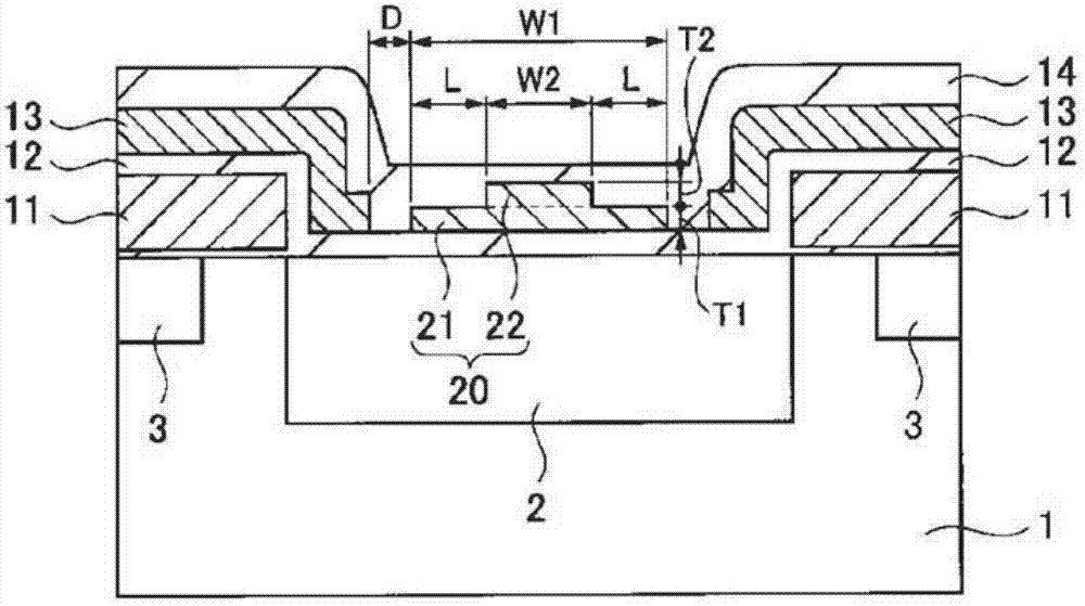
A solid-state imaging element includes a light receiving unit formed on a semiconductor base, and an anti-reflection film formed on the light receiving unit. The anti-reflection film has a plurality of planar layers whose planar layer in an upper layer is narrower than the planar layer in a lower layer.
Description
technical field [0001] The present invention relates to a solid-state imaging element and electronic equipment having the solid-state imaging element. Background technique [0002] In the past, solid-state imaging elements employ a configuration in which an antireflection film is provided on a portion of a semiconductor base where a light receiving unit is formed for suppressing reflection of light at an interface between a semiconductor base such as a silicon substrate and an insulating film thereon resulting in decreased sensitivity. [0003] However, when the light incident on the semiconductor base is incident on the end of the anti-reflection film from an oblique direction, the light passes through the anti-reflection film, and then, a part of the light is not incident on the light receiving unit, but on the surface of the semiconductor base reflective and directed to the outside of the anti-reflective film. As a result, this tends to cause problems such as smear phen...
Claims
Login to View More Application Information
Patent Timeline
 Patent Type & Authority Applications(China)
IPC IPC(8): H01L27/146G02B1/11G02B1/115H01L27/14
CPCH01L27/14806H01L27/14818H01L27/1462H01L27/14629H01L31/0232
Inventor 桝田佳明本渡惠太
Owner SONY SEMICON SOLUTIONS CORP
Features
- Generate Ideas
- Intellectual Property
- Life Sciences
- Materials
- Tech Scout
- Unparalleled Data Quality
- Higher Quality Content
- 60% Fewer Hallucinations
Learn More Browse by: Latest US Patents, China's latest patents, Technical Efficacy Thesaurus, Application Domain, Technology Topic, Popular Technical Reports.
© 2025 PatSnap. All rights reserved.Legal|Privacy policy|Modern Slavery Act Transparency Statement|Sitemap|About US| Contact US: help@patsnap.com