Method of determining gap size in manufacturing single crystal silicon and method of manufacturing single crystal silicon
A technology of gap size and single crystal silicon, which is applied in the directions of single crystal growth, single crystal growth, chemical instruments and methods, etc., and can solve the problems such as the inability to obtain single crystal silicon.
- Summary
- Abstract
- Description
- Claims
- Application Information
AI Technical Summary
Problems solved by technology
Method used
Image

Examples
Embodiment approach
[0055] [Manufacturing method of single crystal silicon]
[0056] Next, a method for producing a silicon single crystal SM according to one embodiment of the present invention will be described.
[0057] It should be noted that, in this embodiment, the case of producing a single crystal silicon SM having a diameter of 300 mm in the straight portion after cylindrical grinding is exemplified, but the diameter after cylindrical grinding may be 200 mm, 450 mm, or other sizes. In addition, a dopant for adjusting the resistivity may be added to the silicon melt M, or may not be added.
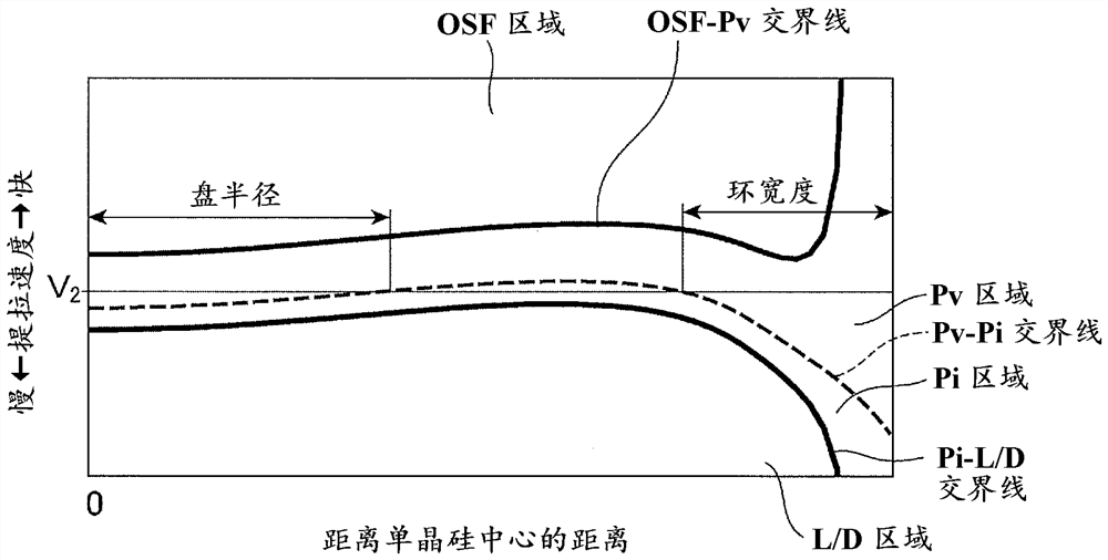
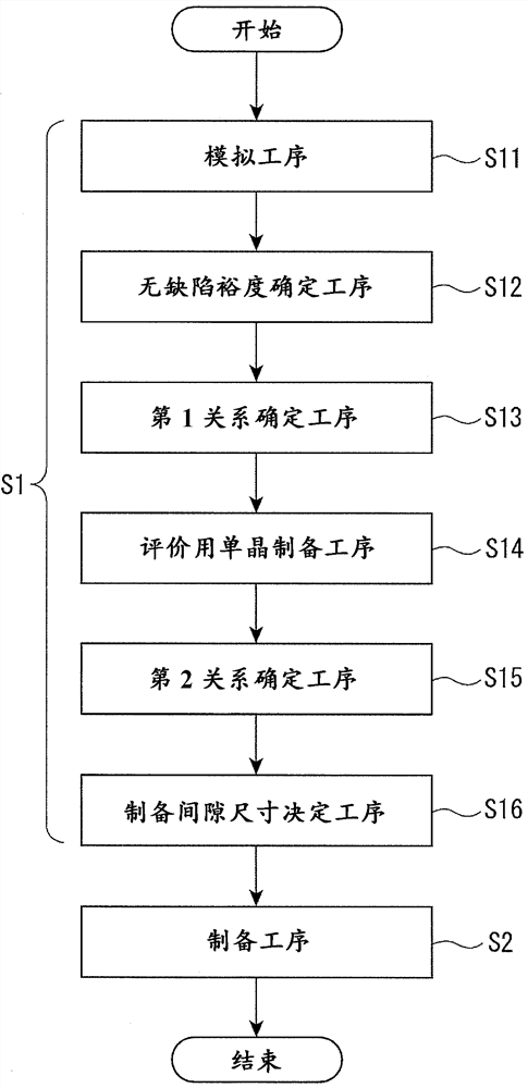
[0058] like figure 2 As shown, in the production method of single crystal silicon SM, the process of implementing the method of determining the gap size when producing single crystal SM SM (step S1), and using the production gap size determined by the determination method to prepare single crystal silicon for products The process of SM (step S2: preparation process). Each step will be described i...
Embodiment
[0105] Next, the present invention will be described in more detail by way of examples and comparative examples, but the present invention is not limited by these examples.
[0106] [Experiment 1]
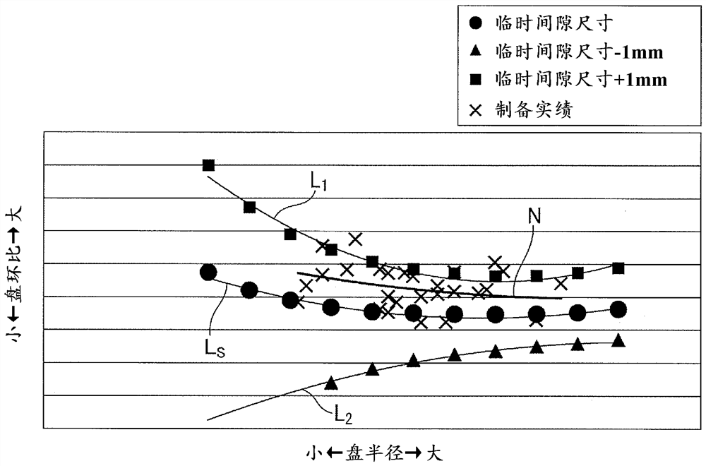
[0107] Based on the above implementation in the Figure 7 A plurality of single-crystal silicon SMs for evaluation were prepared in such a way that ring-shaped and disk-shaped OSF regions were formed with the determined preparation gap size. Then, the disk radii and disk ratios of the plurality of wafers obtained from the silicon single crystal SM for evaluation were obtained, and their relationship was plotted as Image 6 shown in the figure.
[0108] show the results in Figure 9 middle.
[0109] like Figure 9 As shown, the actual approximate line N can be confirmed based on the measurement results of the evaluation single crystal silicon SM prepared with the gap size 1 It is closer to the reference approximation line L than the actual approximation line N of the single cr...
Embodiment 1
[0117] {Example 1}
[0118] Based on the occurrence of OSF in the defective wafer obtained from the silicon single crystal SM of Comparative Example 1, the processes of steps S13 to S14 were performed to determine the preparation gap size of the region where the defective wafer was obtained. Then, the single crystal silicon SM of Example 1 was prepared with the gap size using the pulling device 1 with the A-type hot zone. As the pulling speed of the silicon single crystal SM of Example 1, the same speed as that of Comparative Example 1 was employed.
[0119]Then, the product area of the silicon single crystal SM of Example 1 was determined, and the yield of Example 1 was obtained in the same manner as in Comparative Example 1.
PUM
 Abstract
Description
Claims
Application Information
 - R&D
- Intellectual Property
- Life Sciences
- Materials
- Tech Scout
- Unparalleled Data Quality
- Higher Quality Content
- 60% Fewer Hallucinations
Browse by: Latest US Patents, China's latest patents, Technical Efficacy Thesaurus, Application Domain, Technology Topic, Popular Technical Reports.
© 2025 PatSnap. All rights reserved.Legal|Privacy policy|Modern Slavery Act Transparency Statement|Sitemap|About US| Contact US: help@patsnap.com