Silicon IC-gallium nitride hybrid drive system

A hybrid drive and gallium nitride technology, applied in information technology support systems, electric vehicle charging technology, pulse technology, etc., can solve the problems of limited analog circuit functions, insufficient gate pads, and low maturity

Pending Publication Date: 2020-10-20
苏州量芯微半导体有限公司
View PDF0 Cites 1 Cited by
  • Summary
  • Abstract
  • Description
  • Claims
  • Application Information

AI Technical Summary

Problems solved by technology

[0005] The existing monolithic integrated gallium nitride IC, because the maturity of gallium nitride process technology itself is not high, lack of CMOS logic commonly used in silicon analog circuits (currently there is no p-type high electron mobility tube (P- type HEMT), only the combination of depletion-mode HEMT and enhanced-mode HEMT can be used), this shortcoming leads to the limited functions of GaN monolithic integrated analog circuits, the lack of some necessary functional units, and the inability to achieve some more complex protection and control circuit
At the same time, in terms of unit wafer area, the price of gallium nitride far exceeds that of silicon, and the current process node (minimum line width size) of gallium nitride is much larger than that of silicon, resulting in high monolithic integration costs of gallium nitride
[0006] Although the existing co-packaging method takes advantage of the advantages of mature silicon-based analog circuits, because the silicon IC chip and the GaN chip need to be connected by wire bonding, although the wire diameter is very short, there is still unavoidable parasitic inductance.
Especially when the output pads of silicon IC chips or the gate pads of GaN devices are not large enough to make thicker copper / gold wires, the resulting parasitic inductance cannot be ignored

Method used


Image

  • Silicon IC-gallium nitride hybrid drive system
  • Silicon IC-gallium nitride hybrid drive system
  • Silicon IC-gallium nitride hybrid drive system

Examples


Embodiment Construction

[0029] The following will clearly and completely describe the technical solutions in the embodiments of the present invention with reference to the accompanying drawings in the embodiments of the present invention. Obviously, the described embodiments are only some, not all, embodiments of the present invention. Based on the embodiments of the present invention, all other embodiments obtained by persons of ordinary skill in the art without making creative efforts belong to the protection scope of the present invention.

[0030] It should be noted that in the description of the present invention, terms such as "first" and "second" are only used to describe the purpose and distinguish similar objects, there is no sequence between the two, and they cannot be interpreted as indicating or imply relative importance. In addition, in the description of the present invention, unless otherwise specified, "plurality" means two or more.

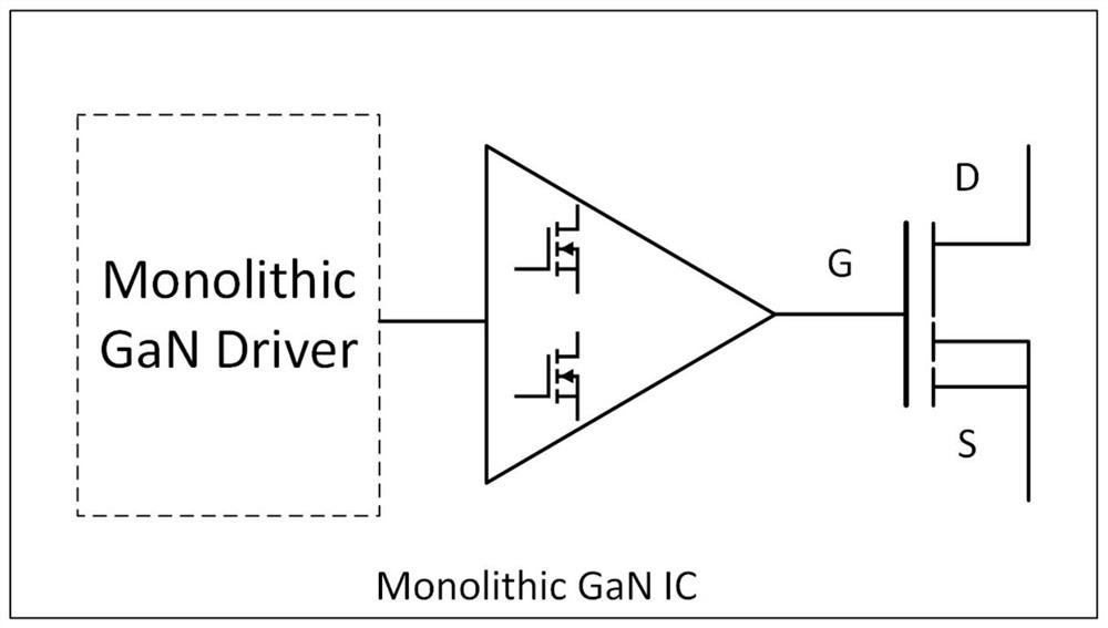
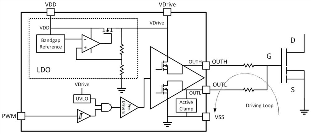
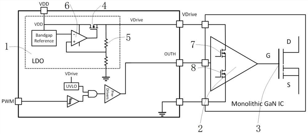
[0031] combine image 3 As shown, this embodimen...


PUM

PropertyMeasurementUnit
lengthaaaaaaaaaa

Abstract

The invention discloses a silicon IC-gallium nitride hybrid driving system. The system comprises a driving module and a gallium nitride power device. The driving module comprises a silicon IC type linear voltage reduction assembly used for outputting a preset voltage and a gallium nitride monolithic integrated type driving half-bridge assembly. The output end of the gallium nitride monolithic integrated drive half-bridge assembly is in signal connection with a gate circuit of the gallium nitride power device, so as to modulate the conductivity of the gallium nitride power device in a chargingand discharging manner. The silicon IC type linear voltage reduction assembly is connected with the gallium nitride monolithic integrated type drive half-bridge assembly through wire bonding; and thedriving module and the gallium nitride power device are matched in a common packaging mode. The system at least comprises the following advantages: the advantages of flexibility, low cost and maturityof a silicon IC integrated circuit and the advantages of a gallium nitride monolithic integrated half-bridge assembly for eliminating parasitic parameters of a drive circuit are combined.

Description

technical field [0001] The invention relates to the technical fields of power electronics and power semiconductors, in particular to a silicon IC-gallium nitride hybrid drive system. Background technique [0002] The statements in this section only provide background information related to the present disclosure and may not constitute prior art. [0003] Gallium nitride is known as the representative material of the third generation of semiconductors. It has achieved mass production in the field of small and medium power adapters, and it is expected to fully replace silicon in some fields in the near future. However, the application of gallium nitride power devices requires corresponding gate driver chips, and ordinary silicon power device driver chips cannot be directly applied to gallium nitride power devices, because the performance requirements such as driving voltage and driving capability are different. [0004] At present, gallium nitride power devices are mainly in ...

Claims


Application Information

Patent Timeline
Patent Type & Authority Applications(China)
IPC IPC(8): H03K17/56
CPCH03K17/56H03K2217/0081Y04S30/12Y02T90/167
Inventor 傅玥李湛明吴伟东刘雁飞
Owner 苏州量芯微半导体有限公司
Why Eureka
Try Eureka