A method for smelting silicon wafer cutting waste under slight negative pressure
A silicon wafer cutting and micro-negative pressure technology, which is applied in chemical instruments and methods, silicon compounds, inorganic chemistry, etc., can solve the problems of lengthy process, low impurity removal rate, and difficulty in precise control of participation.
- Summary
- Abstract
- Description
- Claims
- Application Information
AI Technical Summary
Problems solved by technology
Method used
Image
Examples
Embodiment 1
[0028] Embodiment 1: A kind of method for smelting silicon wafer cutting waste under slight negative pressure, the specific steps are as follows:
[0029] (1) The silicon wafer cutting waste in a certain place in Yunnan is subjected to induction melting, so that the bulk powder is melted into a high-temperature silicon liquid; in terms of mass percentage, the impurity content in the silicon wafer cutting waste is 6000ppm for Al and 3000ppm for Ca;
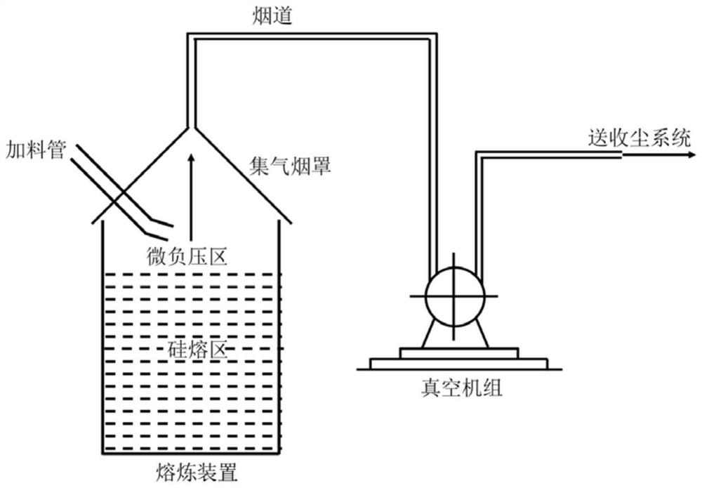
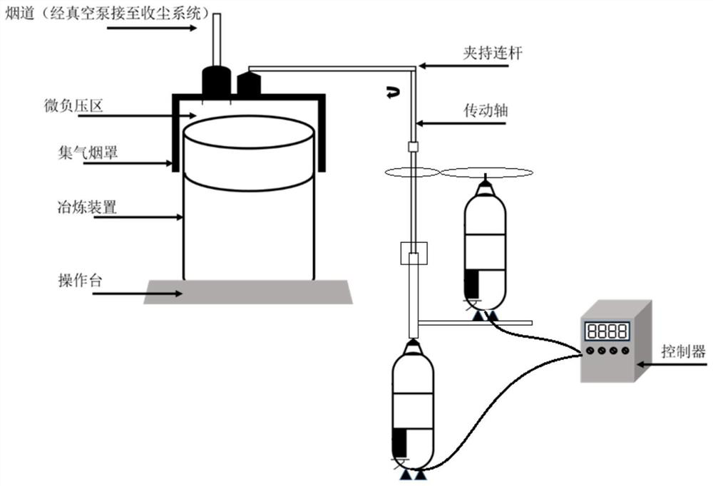
[0030](2) In order to further reduce Al and Ca, at the same time as step (1) induction smelting, micro-negative pressure smelting is carried out, and the fume collecting hood of the micro-negative pressure device is moved to the furnace mouth of the smelting device (induction furnace) through the lifting-rotating member Right above, so that the mouth of the fume collecting hood can cover the mouth of the furnace, and the vacuum device of the micro-negative pressure device (two-cascade mechanical vacuum pump) is turned on. The silico...
Embodiment 2
[0033] Embodiment 2: A kind of method for smelting silicon wafer cutting waste under slight negative pressure, the specific steps are as follows:
[0034] (1) The silicon wafer cutting waste in a certain place in Yunnan is subjected to induction melting, so that the bulk powder is melted into a high-temperature silicon liquid; in terms of mass percentage, the impurity content in the silicon wafer cutting waste is 11000ppm for Al and 3000ppm for Ca;
[0035] (2) In order to further reduce Al and Ca, carry out slagging smelting to the high-temperature silicon liquid of step (1) induction smelting; wherein the slagging agent is CaO, and the addition amount of CaO is 2kg / ton based on the quality of silicon chip cutting waste ; After adding the slagging agent CaO, pass through industrial compressed nitrogen, and the ventilation time is about 15 minutes;
[0036] (3) Carry out micro-negative pressure smelting while slagging and smelting in step (2), and move the fume-collecting hood...
Embodiment 3
[0039] Embodiment 3: A kind of method for smelting silicon wafer cutting waste under slight negative pressure, the specific steps are as follows:
[0040] (1) The silicon wafer cutting waste in a certain place in Yunnan is subjected to induction melting, so that the bulk powder is melted into a high-temperature silicon liquid; in terms of mass percentage, the impurity content in the silicon wafer cutting waste is 8000ppm for Al and 500ppm for Ca;
[0041] (2) In order to further reduce Al and Ca, the high-temperature silicon liquid induced in step (1) is subjected to combined smelting by gas blowing and slagging; the gas blowing is top blowing ventilation, the gas is industrial oxygen, and the ventilation time is about 10 minutes. The pressure is 1.2-2 atmospheres, and the gas flow rate is 0.2-1m 3 / s; the slagging agent is CaO, and the amount of CaO added is 1kg / ton based on the quality of silicon wafer cutting waste;
[0042] (3) Micro-negative pressure smelting is carried ...
PUM
 Abstract
Description
Claims
Application Information
 - R&D
- Intellectual Property
- Life Sciences
- Materials
- Tech Scout
- Unparalleled Data Quality
- Higher Quality Content
- 60% Fewer Hallucinations
Browse by: Latest US Patents, China's latest patents, Technical Efficacy Thesaurus, Application Domain, Technology Topic, Popular Technical Reports.
© 2025 PatSnap. All rights reserved.Legal|Privacy policy|Modern Slavery Act Transparency Statement|Sitemap|About US| Contact US: help@patsnap.com


