SCR electrostatic protection structure and forming method thereof

A technology of electrostatic protection and conductive structure, applied in the direction of circuits, electrical components, electrical solid devices, etc., can solve problems such as poor performance

Active Publication Date: 2020-10-16
SEMICON MFG INT (SHANGHAI) CORP +1
View PDF7 Cites 1 Cited by
  • Summary
  • Abstract
  • Description
  • Claims
  • Application Information

AI Technical Summary

Problems solved by technology

[0004] However, the performance of existing ESD protection structures is poor

Method used


Image

  • SCR electrostatic protection structure and forming method thereof
  • SCR electrostatic protection structure and forming method thereof
  • SCR electrostatic protection structure and forming method thereof

Examples


Embodiment Construction

[0029] As mentioned in the background, semiconductor devices formed in the prior art have poor performance.

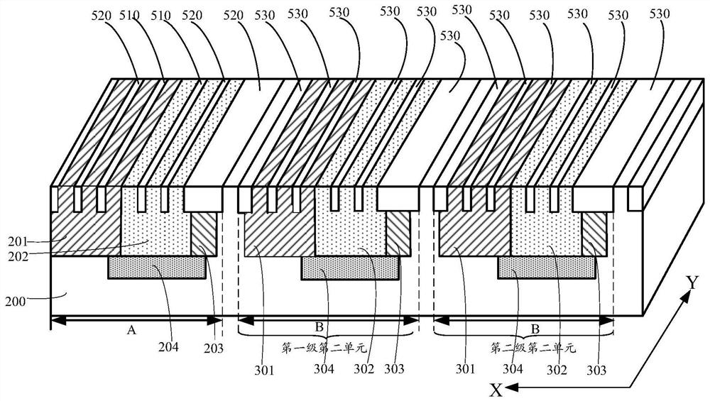
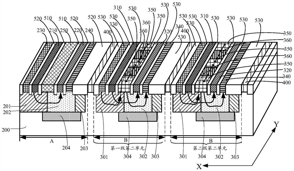
[0030] There are two important parameters in the SCR electrostatic protection structure, namely holding voltage and trigger voltage. Higher holding voltage and lower triggering voltage are the process directions that SCR electrostatic protection structures are constantly pursuing.

[0031] The existing SCR electrostatic protection structure includes: a P-type semiconductor substrate; an SCR unit located in the semiconductor substrate; the SCR unit includes: a first N-type well located in the semiconductor substrate; a first N-type well located in the first N-type well P-type well, the first P-type well is located on the side of the first N-type well and adjacent to the first N-type well; the second N-type well surrounding the first P-type well and the first N-type well; located in the first N-type well The P-type doped region at the top of the first P-type well; the N...


PUM


Abstract

The invention discloses an SCR electrostatic protection structure and a forming method thereof. The structure comprises: a first unit and a second unit, wherein the first unit comprises a first P-typedoped region positioned at the top in a first N-type well, and a first N-type doped region positioned at the top in a first P-type well, and the second unit comprises a second P-type doped region positioned at the top in a second N-type well, and a second N-type doped region and a third P-type doped region which are located at the top in a second P-type well; a bridging doping group, wherein thebridging doping group comprises a plurality of fourth P-type doped regions arranged along a second direction, each fourth P-type doped region is located at the top of part of the second N-type well and extends to the top of part of the second P-type well, the second direction is perpendicular to the first direction, and a fourth N-type doped region is arranged between the adjacent fourth P-type doped regions; and a conductive structure electrically connected with the fourth N-type doped region and the fourth P-type doped region. According to the invention, the performance of the SCR electrostatic protection structure is improved.

Description

technical field [0001] The invention relates to the field of electrostatic protection, in particular to an SCR electrostatic protection structure and a forming method thereof. Background technique [0002] In the production and application of integrated circuit chips, with the continuous improvement of VLSI process technology, the current CMOS integrated circuit production technology has entered the deep submicron stage, the size of MOS devices is continuously reduced, and the thickness of the gate oxide layer is getting higher and higher. Thinner and thinner, the withstand voltage capability of MOS devices is significantly reduced, and the harm of electrostatic discharge (Electrostatic Discharge, ESD) to integrated circuits has become more and more significant. Therefore, ESD protection for integrated circuits becomes particularly important. [0003] In order to strengthen the protection against static electricity, an electrostatic protection circuit is usually connected t...

Claims


Application Information

Patent Timeline
IPC IPC(8): H01L27/02H01L21/82
CPCH01L27/0262H01L27/0296H01L21/82
Inventor 杜飞波
Owner SEMICON MFG INT (SHANGHAI) CORP
Why Eureka
Try Eureka