Crucible for casting monocrystalline silicon and method for casting monocrystalline silicon
A monocrystalline silicon and crucible technology, applied in the field of photovoltaics, can solve problems such as high cost and affecting crystal quality, reduce the proportion of miscellaneous crystals, and improve the success rate of protection retention
- Summary
- Abstract
- Description
- Claims
- Application Information
AI Technical Summary
Problems solved by technology
Method used
Image
Examples
Embodiment Construction
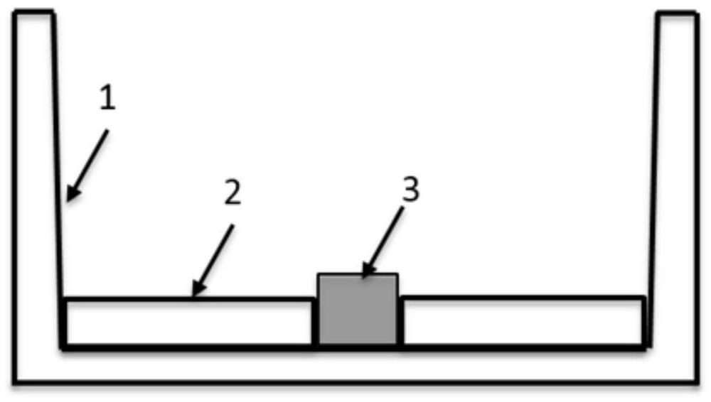
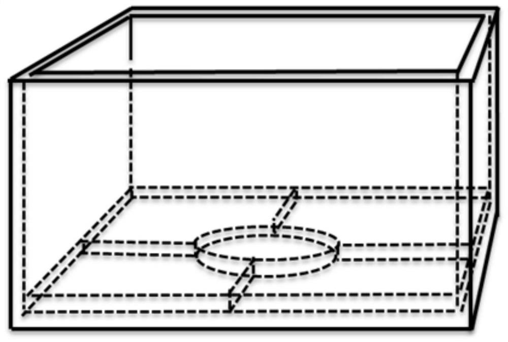
[0021] Such as figure 1 and figure 2 As shown, the present invention includes a crucible body 1, and also includes a backing plate 2 laid on the inner bottom of the crucible body 1, and the backing plate 2 has a seed crystal notch 3 that matches the shape of the single crystal silicon seed crystal, wherein , the seed crystal notch 3 is located in the middle of the backing plate 2 . The seed crystal notch 3 is in the shape of a cylinder or a truncated cone. In the present invention, a cylindrical seed crystal cut from a single wafer bar can be used, without cutting the cylindrical seed crystal into a square seed crystal.
[0022] Such as figure 1 and figure 2 As shown, the backing plate 2 in the present invention can be spliced by at least two backing plates, for example, four backing plates can be used, and a gap is provided on the backing plate, and when each backing plate splicing pad is arranged on the inner bottom of the crucible body 1, The gaps of the various ba...
PUM
 Abstract
Description
Claims
Application Information
 - R&D Engineer
- R&D Manager
- IP Professional
- Industry Leading Data Capabilities
- Powerful AI technology
- Patent DNA Extraction
Browse by: Latest US Patents, China's latest patents, Technical Efficacy Thesaurus, Application Domain, Technology Topic, Popular Technical Reports.
© 2024 PatSnap. All rights reserved.Legal|Privacy policy|Modern Slavery Act Transparency Statement|Sitemap|About US| Contact US: help@patsnap.com


