
Processing method and device

A processing method and a technology of a processing device, which are applied to TVs, solid-state image signal generators, color TV components, etc., can solve the problems of slow real-time image processing speed, insufficient bandwidth for accessing DDR at the PL end, slowing down the conversion rate, etc. Achieve the effect of optimizing display processing, improving image processing and display speed, and increasing frame rate

Inactive Publication Date: 2020-10-13
深兰人工智能芯片研究院(江苏)有限公司
View PDF3 Cites 0 Cited by
  • Summary
  • Abstract
  • Description
  • Claims
  • Application Information

AI Technical Summary

Problems solved by technology

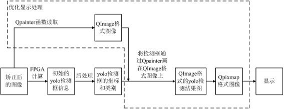
[0005] The above-mentioned pre-processing flow and display processing flow have the following disadvantages: (1) Both the PS end and the PL end need to access the DDR, but because the PL end accesses the DDR too frequently, the bandwidth of the PL end accessing the DDR is not enough; (2) due to the mat transfer The QImage format is a pixel-level conversion, which requires a huge amount of calculation. For example, for an image with a resolution of 1080*720, the conversion requires millions of calculations, and the fastest time-consuming is about 100ms, which seriously slows down the overall conversion rate.
The above shortcomings lead to the slow real-time processing of images, and the number of frames cannot meet the real-time frame rate requirements

Method used


Image

  • Processing method and device
  • Processing method and device
  • Processing method and device

Examples


Embodiment Construction

[0024] The following will clearly and completely describe the technical solutions in the embodiments of the present invention with reference to the accompanying drawings in the embodiments of the present invention. Obviously, the described embodiments are only some, not all, embodiments of the present invention. Based on the embodiments of the present invention, all other embodiments obtained by persons of ordinary skill in the art without making creative efforts belong to the protection scope of the present invention.

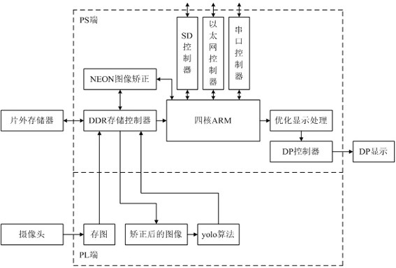
[0025] The processing method and device of the embodiment of the present invention are based on figure 2 The improved FPGA+ARM architecture shown is implemented. In the FPGA+ARM architecture, the PS side includes a quad-core ARM, and the quad-core ARM is connected to necessary controllers such as SD controllers, Ethernet controllers, and serial port controllers. PS The memory at the end includes the DDR storage controller and its connected off-chip memory; th...


PUM


Abstract

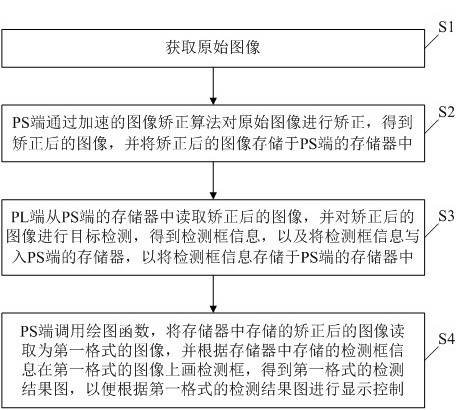
The invention provides a processing method and device. The method comprises the following steps: acquiring an original image; the PS end correctings the original image through an accelerated image correction algorithm via a PS end to obtain a corrected image, and storinges the corrected image in a memory of the PS end; the PL end readings the corrected image from the memory of the PS end via a PLend, performings target detection on the corrected image to obtain detection frame information, and writinges the detection frame information into the memory of the PS end to store the detection frameinformation into the memory of the PS end; and the PS terminal callings a drawing function via the PS end, readings the corrected image stored in the memory as an image in a first format, and drawings a detection frame on the image in the first format according to the detection frame information stored in the memory to obtain a detection result graph in the first format, so as to perform displaycontrol according to the detection result graph in the first format. According to the method disclosed in the invention, the image processing and displaying speed can be effectively improved, so thatand therefore the frame rate of dynamic images or videos is improved.

Description

technical field [0001] The present invention relates to the technical field of image processing, in particular to a processing method and a processing device. Background technique [0002] Based on the FPGA (Field Programmable Gate Array, field programmable logic gate array) + ARM (Advanced RISC Machine, a microprocessor) architecture, the display of dynamic images or videos with detection frames generally includes pre-processing and display processing. [0003] Among them, the pre-processing process mainly performs image distortion correction and acquisition of detection frame data. The pre-processing process specifically includes: storing the original image captured by the camera in ARM, that is, DDR (Double Data Rate SDRAM, double-rate synchronous dynamic random access memory) on the PS (Processing System, processing system) side, and then taking it out to FPGA , that is, the PL (Progarmmable Logic, programmable logic) terminal, the corrected image is obtained after imag...

Claims


Application Information

Patent Timeline
Patent Type & Authority Applications(China)
IPC IPC(8): H04N5/357H04N9/04
CPCH04N25/61H04N23/10
Inventor 陈海波
Owner 深兰人工智能芯片研究院(江苏)有限公司
Learn More