A wafer automatic brushing machine

An automatic brushing and wafer technology, applied in the direction of cleaning methods using liquids, cleaning methods and utensils, chemical instruments and methods, etc., can solve the problems of affecting the quality of wafers, easily scratching wafers, and low scrubbing efficiency, and achieve Clean and thorough scrubbing, improve scrubbing effect, and improve scrubbing efficiency

Active Publication Date: 2020-12-01
SHANDONG NOVOSHINE OPTOELECTRONICS CO LTD
View PDF6 Cites 0 Cited by
  • Summary
  • Abstract
  • Description
  • Claims
  • Application Information

AI Technical Summary

Problems solved by technology

[0005] Specifically, the technical problem to be solved by the present invention is to provide an automatic wafer brushing machine to solve the problem of manual single-chip scrubbing of wafers at present, which has low scrubbing efficiency, high labor intensity, and is easy to scratch the wafer, which affects Wafer Quality Technical Issues

Method used


Image

  • A wafer automatic brushing machine
  • A wafer automatic brushing machine
  • A wafer automatic brushing machine

Examples


Embodiment Construction

[0068] The present invention will be further described below in conjunction with specific examples. However, the uses and purposes of these exemplary embodiments are only used to illustrate the present invention, and do not constitute any form of limitation to the actual protection scope of the present invention, nor limit the protection scope of the present invention thereto.

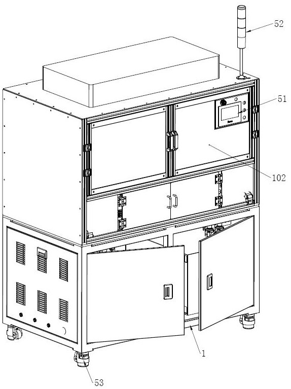
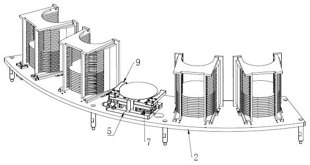
[0069] Such as Figure 1 to Figure 15 Commonly shown, the present embodiment provides a wafer automatic chip brushing machine, including a frame 1, a workbench 101 is provided on the frame 1, a material rack 2 is provided on the workbench 101, and several The flower basket is placed, and a wafer positioning mechanism is provided in the middle of the rack 2 .

[0070] A mechanical arm 11 corresponding to the material rack 2 is also installed on the workbench 101. A wafer pallet 13 is mounted on the execution end of the mechanical arm 11. The end of the wafer pallet 13 has a wafer holding part 1301. A ...


PUM


Abstract

The invention belongs to the technical field of wafer production and processing, and provides an automatic wafer scrubbing machine, which comprises a rack, wherein a workbench is arranged on the rack,a material frame is arranged on the workbench, a plurality of basket placing positions are arranged on the material frame, a wafer positioning mechanism is arranged in the middle of the material frame, a mechanical arm is further installed on the workbench, a wafer supporting plate is installed at the executing end of the mechanical arm, the two sides of the mechanical arm are respectively provided with a wafer scrubbing box, one side of each wafer scrubbing box is provided with a wafer taking and placing opening, a vacuum pipe driven by a first driving device and a second driving device is arranged below the workbench, a Bernoulli suction disc is installed at the top end of the vacuum pipe, an upper installation plate driven by a third driving device and a fourth driving device is arranged on the workbench, and a sponge brush head driven by a fifth driving device is rotationally installed at the end, located in the wafer scrubbing box, of the upper installation plate. According to the automatic wafer scrubbing device, automatic scrubbing of wafers is achieved, the scrubbing efficiency is greatly improved, scrubbing is clean and thorough, secondary pollution and scratches cannot be caused to the wafer, and it is guaranteed that the quality and the percent of pass of the wafer are not affected.

Description

technical field [0001] The invention relates to the technical field of wafer production and processing, in particular to an automatic wafer brushing machine. Background technique [0002] Wafer refers to the silicon wafer used to make silicon semiconductor integrated circuits. Because of its circular shape, it is called a wafer. With the continuous shrinking of the critical dimensions of semiconductor devices and the introduction of new materials, during the production and processing of wafers, the requirements for the cleanliness of the wafer surface are becoming more and more stringent, and multiple cleanings are usually required to remove Attached dirt and process fluid. [0003] At present, the cleaning of wafers is usually divided into two methods: tank cleaning and single-chip cleaning; tank cleaning is to put the wafer in the cleaning tank for cleaning, which can realize the cleaning of several wafers at the same time, with high cleaning efficiency , but the cleanin...

Claims


Application Information

Patent Timeline
Patent Type & Authority Patents(China)
IPC IPC(8): H01L21/67H01L21/68H01L21/683B08B1/00B08B1/02B08B3/02B08B3/08
CPCB08B1/006B08B1/02B08B3/022B08B3/08H01L21/67046H01L21/67051H01L21/68H01L21/6838
Inventor 郭明灿李凯杰赵成浩王子龙
Owner SHANDONG NOVOSHINE OPTOELECTRONICS CO LTD
Why Eureka
Try Eureka