Display panel and preparation method thereof

A technology for display panels and substrates, which is used in semiconductor/solid-state device manufacturing, identification devices, instruments, etc., and can solve problems such as inability to print

Active Publication Date: 2020-09-29
WUHAN CHINA STAR OPTOELECTRONICS SEMICON DISPLAY TECH CO LTD
View PDF7 Cites 1 Cited by
  • Summary
  • Abstract
  • Description
  • Claims
  • Application Information

AI Technical Summary

Problems solved by technology

[0003] This application provides a display panel and its preparation method to solve the problem that printing cannot be performed because the contact angle between the ink and the black matrix layer is too small

Method used


Image

  • Display panel and preparation method thereof
  • Display panel and preparation method thereof
  • Display panel and preparation method thereof

Examples


Embodiment Construction

[0033] The following will clearly and completely describe the technical solutions in the embodiments of the application with reference to the drawings in the embodiments of the application. Apparently, the described embodiments are only some of the embodiments of the application, not all of them. Based on the embodiments in this application, all other embodiments obtained by those skilled in the art without making creative efforts belong to the scope of protection of this application.

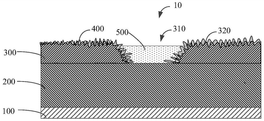
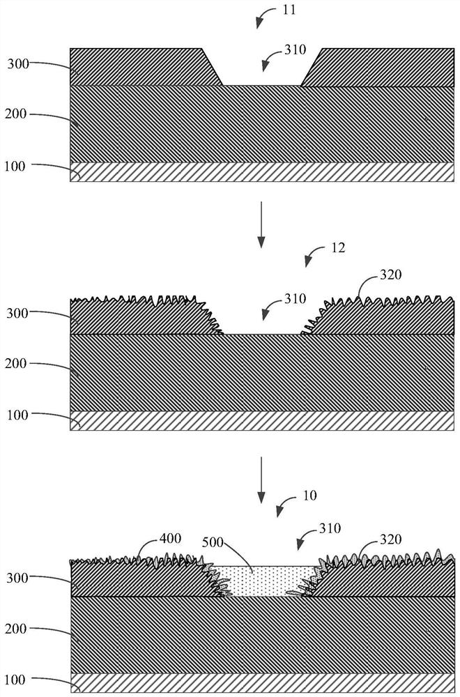
[0034] see figure 1 , figure 1 A cross-sectional view of the structure of the display panel provided in this application. The present application provides a display panel 10 . The display panel 10 includes a substrate 100 , an encapsulation layer 200 , a black matrix layer 300 and an oil-repellent layer 400 .

[0035] The substrate 100 includes a glass substrate, a resin substrate, a quartz substrate, and the like.

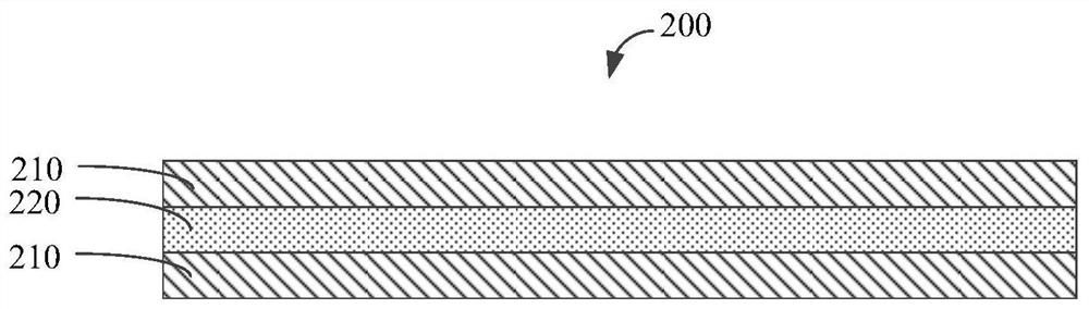
[0036] see figure 2 , figure 2 It is a cross-sectional view of the str...


PUM


Abstract

The invention provides a display panel and a preparation method thereof. The display panel comprises a substrate, a packaging layer, a black matrix layer and an oleophobic layer, the packaging layer is arranged on the surface of the substrate, the black matrix layer is arranged on the packaging layer, the black matrix layer comprises through holes, the through holes penetrate through the black matrix layer to expose the packaging layer, and the oleophobic layer covers the black matrix layer. According to the application, the oleophobic layer is arranged on the black matrix layer, so that the contact angle between the photoresist liquid drop and the interface of the through hole is increased, and the ink effectively flows into the through hole and forms a film uniformly in the printing process.

Description

technical field [0001] The present application relates to the field of display technology, in particular to a display panel and a manufacturing method thereof. Background technique [0002] Due to the low transmittance, large thickness, brittle texture and high price of the polarizer itself, the application of flexible OLED display technology is greatly limited. Therefore, a method of manufacturing color filters instead of circular polarizers on thin film packaging is proposed. However, inkjet printing technology is usually used to prepare color filters on packaging films. The color filters prepared by inkjet printing technology have a simple process, no photolithography mask is needed in the production process, and the material utilization rate is high. When the photoresist droplets are printed into the pixel pits, the contact angle between the ink and the black matrix layer is too small, so that the printing cannot be performed. Contents of the invention [0003] The p...

Claims


Application Information

Patent Timeline
Patent Type & Authority Applications(China)
IPC IPC(8): H01L51/52H01L27/32G09F9/30
CPCG09F9/301H10K59/12H10K50/84H10K50/865H10K50/844C08L1/284C09D133/26H10K50/86H10K71/00C09D7/63C08K5/098C09D101/288C09D139/02C09D147/00H10K59/38H10K50/841
Inventor 龚文亮鲜于文旭
Owner WUHAN CHINA STAR OPTOELECTRONICS SEMICON DISPLAY TECH CO LTD
Why Eureka
Try Eureka