Tunable laser and manufacturing method thereof

A technology for tuning lasers and light spots, which is applied to lasers, laser components, semiconductor lasers, etc., can solve the problems of inability to change the shape of the mode field, increase the cost of packaging, and mismatch the mode field, so as to reduce the power density and increase the output power , reducing the effect of overlap

Active Publication Date: 2020-09-25
INST OF SEMICONDUCTORS - CHINESE ACAD OF SCI
View PDF8 Cites 3 Cited by
  • Summary
  • Abstract
  • Description
  • Claims
  • Application Information

AI Technical Summary

Problems solved by technology

When the light of the semiconductor active device is directly coupled into the optical fiber or the light transmitted by the optical fiber is coupled into the semiconductor active device, the coupling loss may be as high as 10dB due to the mismatch of the mode field between the optical fiber and the semiconductor active device
The coupling efficiency between them can be improved by using lenses or tapered fibers, but these solutions still have the problem of mode field mismatch
These solutions can only change the size of the mode field but cannot change the shape of the mode field, and the alignment tolerance is small, which undoubtedly increases the packaging cost

Method used


Image

  • Tunable laser and manufacturing method thereof
  • Tunable laser and manufacturing method thereof
  • Tunable laser and manufacturing method thereof

Examples


Embodiment 1

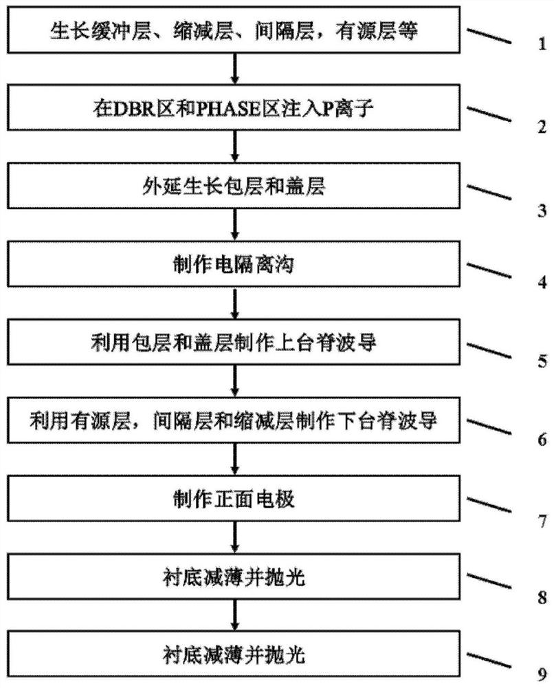
[0071] The invention provides a method for manufacturing a tunable laser, such as figure 1 shown, including the following steps:

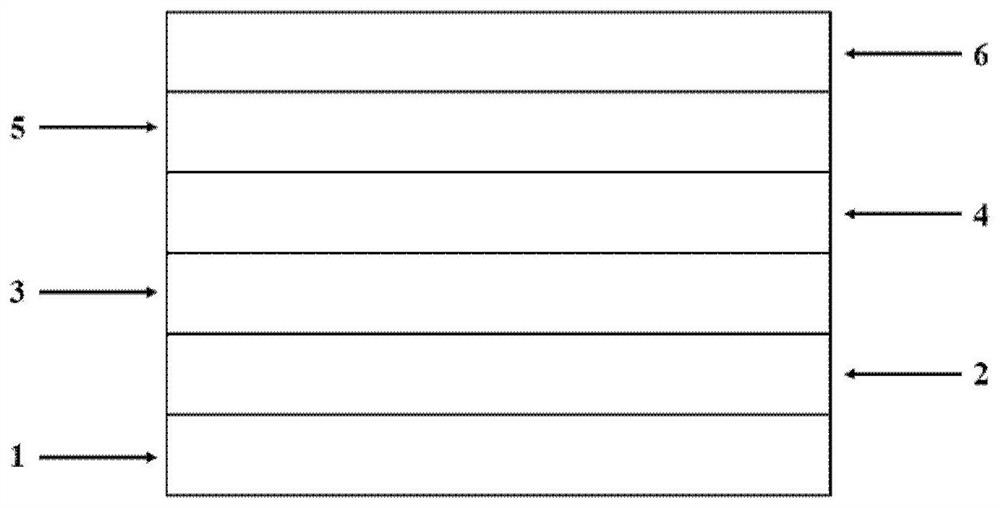
[0072] Step 1: epitaxially grow n-type InP buffer layer 2 (500nm thick), spot enlargement layer 3, and InP spacer layer 4 ( 1.5-2.5μm thick), InGaAlAs active layer 5 (including InAlAs upper and lower confinement layers and InGaAlAs quantum well layers, 200nm-300nm thick) and InP sacrificial layer 6 (300nm thick), such as figure 2 ;

[0073] Wherein, the spot enlargement layer 3 is a far-field reduction layer formed of an InGaAsP layer with a thickness of 40-60 nm;

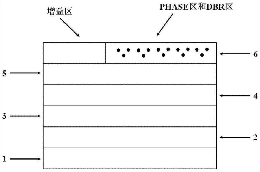
[0074] Step 2: Use ion implantation equipment to implant P ions into the InP sacrificial layer 6 in the DBR region and the phase region to introduce a large number of point defects, and rapid thermal annealing to move the point defects to the InGaAlAs active layer 5 to promote the quantum of the InGaAlAs active layer 5 The interdiffusion of elements in the well and the quantum barri...

Embodiment 2

[0083] The preparation method of this embodiment 2 is the same as that of embodiment 1, the difference is that the light spot amplification layer 3 of this embodiment 2 is a diluted waveguide layer, and a 60nm-thick InGaAsP layer and a 300nm-thick InP layer are alternately grown for 3 to 5 cycles form.


PUM

PropertyMeasurementUnit
thicknessaaaaaaaaaa

Abstract

The invention discloses a tunable laser and a manufacturing method thereof. The tunable laser comprises a gain region and a distributed Bragg reflection region which are positioned on the same substrate, are equal in height and are attached to each other, wherein the gain region and the distributed Bragg reflection region are respectively of a double-ridge waveguide structure, and each of the gainregion and the distributed Bragg reflection region comprises a lower ridge waveguide and an upper ridge waveguide; the lower ridge waveguide of the gain region and the lower ridge waveguide of the distributed Bragg reflection region respectively and sequentially comprise a light spot amplification layer, a spacing layer and an active layer from bottom to top; the upper ridge waveguide of the gainregion and the upper ridge waveguide of the distributed Bragg reflection region respectively comprise a cladding layer and a cover layer from bottom to top; the upper ridge waveguide of the gain region is a wedge-shaped waveguide; and the upper ridge waveguide of the distributed Bragg reflection region is a side wall grating waveguide. According to the tunable laser, the light spot size of the end face of the laser can be amplified while the wavelength tuning function is achieved, and the coupling efficiency of the laser and the optical fiber is improved.

Description

technical field [0001] The invention relates to the field of optoelectronic devices, in particular to a tunable laser and a manufacturing method thereof. Background technique [0002] As another great invention after computers and semiconductors since the 20th century, laser has the advantages of high brightness, good directionality, and strong coherence. Long-distance, ultra-long-distance, high-speed, ultra-high-speed, and ultra-large-capacity optical fiber communication systems are the needs of the development of modern information society. Whether it is the backbone network and wide area network of long-distance communication, or the local area network of short-distance communication, access network, short-distance data connection optical switching, etc., a large number of high-performance and low-cost optoelectronic devices are required to support the functions of optical networks. Compared with other lasers, semiconductor lasers have the advantages of small size, high ...

Claims


Application Information

Patent Timeline
Patent Type & Authority Applications(China)
IPC IPC(8): H01S5/125H01S5/227H01S5/30
CPCH01S5/125H01S5/2275H01S5/3013
Inventor 剌晓波梁松唐强刘云龙张立晨朱旭愿
Owner INST OF SEMICONDUCTORS - CHINESE ACAD OF SCI
Why Eureka
Try Eureka