Embedded features for interlocks using additive manufacturing

A technology for identifying features and characteristics, applied in the manufacture of components with interlocking and embedded identification features, and in the field of additive manufacturing, it can solve the problem of not being able to judge that the system contains components that meet the expected specifications

Pending Publication Date: 2020-09-22
VARIAN SEMICON EQUIP ASSOC INC
View PDF5 Cites 0 Cited by
  • Summary
  • Abstract
  • Description
  • Claims
  • Application Information

AI Technical Summary

Problems solved by technology

[0005] Unfortunately, in most semiconductor processing systems, it is not possible to tell if the system contains only components that meet the desired specifications
Therefore, after replacing components, the system may no longer perform at its stated level

Method used


Image

  • Embedded features for interlocks using additive manufacturing
  • Embedded features for interlocks using additive manufacturing
  • Embedded features for interlocks using additive manufacturing

Examples


Embodiment Construction

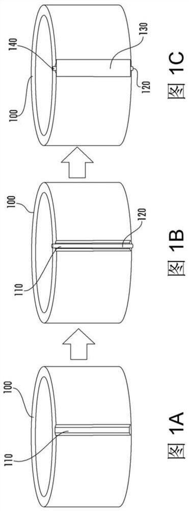
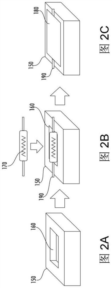
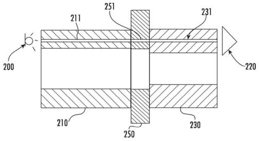
[0021] As mentioned above, a semiconductor manufacturing system may be composed of multiple components. Identification features may be embedded in any or all of these components to allow the system to identify the component. An identification feature can be any element that can be used to identify a component. In some embodiments, the component may be an annular ring, such as a gasket, flange, or other similar component. In other embodiments, the components may be rectangular in shape. Of course, the components can also be of any other shape.

[0022] Figure 1A to Figure 1C The sequence used to embed the identifying features into the assembly is shown. Figure 1A Assembly 100 is shown shaped as an annular ring or hollow cylinder. First, if Figure 1A As shown, cavities 110 may be introduced subtractively into the side walls of component 100 . This cavity 110 may be in the form of a channel in some embodiments. The cavity 110 can be made by grinding, etching or any othe...


PUM


Abstract

The present disclosure describes a method and apparatus for determining whether components in a semiconductor manufacturing system are authorized for use in that system. By embedding an identificationfeature in the component, it is possible for a controller to determine whether that component is qualified for use in the system. Upon detection of an unauthorized component, the system may alert theuser or, in certain embodiments, stop operating of the system. This identification feature is embedded in a component by using an additive manufacturing process that allows the identification featureto be embedded in the component without subjecting the identification feature to extreme temperatures.

Description

technical field [0001] The present disclosure is in the technical field of additive manufacturing, and more specifically, in the technical field of fabricating components with interlocking and embedded identification features. Background technique [0002] Semiconductor devices are fabricated using complex semiconductor processing systems that include many different components. Semiconductor yield and performance depend on the interaction and cooperation of these components. For example, if a component falls below target specifications, the resulting semiconductor device may be adversely affected. [0003] Accordingly, equipment manufacturers attempt to provide high quality components for these complex semiconductor processing systems. The device manufacturer then specifies overall system performance based on the specifications of each component. [0004] Some of the components used in these complex semiconductor systems may wear out with use or wearout. Often, replaceme...

Claims


Application Information

Patent Timeline
IPC IPC(8): H01J37/317H01J37/16
CPCH01L21/67213H01L21/67288H01L21/67294H01J37/3171H01J37/16H01J2237/2482C23C14/48B33Y80/00G08B21/18
Inventor 奎格·R·钱尼亚当·M·麦劳克林
Owner VARIAN SEMICON EQUIP ASSOC INC
Why Eureka
Try Eureka