Semiconductor structure and manufacturing method thereof

A manufacturing method and semiconductor technology, applied in the fields of semiconductor/solid-state device manufacturing, semiconductor devices, electrical components, etc., can solve the problems of many defects in the gallium arsenide film, high noise, large dark current of optoelectronic devices, etc.

Active Publication Date: 2020-09-18
GUANGDONG GREATER BAY AREA INST OF INTEGRATED CIRCUIT & SYST +1
View PDF11 Cites 2 Cited by
  • Summary
  • Abstract
  • Description
  • Claims
  • Application Information

AI Technical Summary

Problems solved by technology

[0002]With the diversification of semiconductor devices, it is necessary to combine multiple semiconductor materials to form semiconductor devices. In some scenarios, gallium arsenide (GaAs) materials need to be used to prepare detectors , lasers, etc., so there is a need to form gallium arsenide thin films on silicon (Si) substrates. However, the lattice mismatch between silicon and gallium arsenide is serious, so epitaxially grown gallium arsenide films on silicon substrates There are many defects, and the antiphase domin (APD) is serious. The optoelectronic devices based on such gallium arsenide film layer have large dark current and high noise. Gallium layer

Method used


Image

  • Semiconductor structure and manufacturing method thereof
  • Semiconductor structure and manufacturing method thereof
  • Semiconductor structure and manufacturing method thereof

Examples


Embodiment Construction

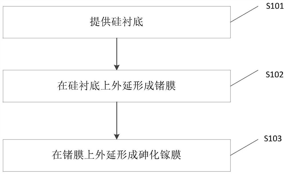
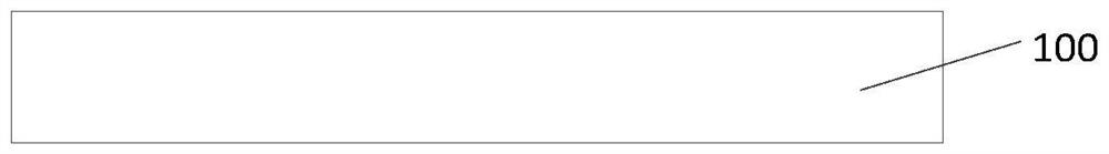
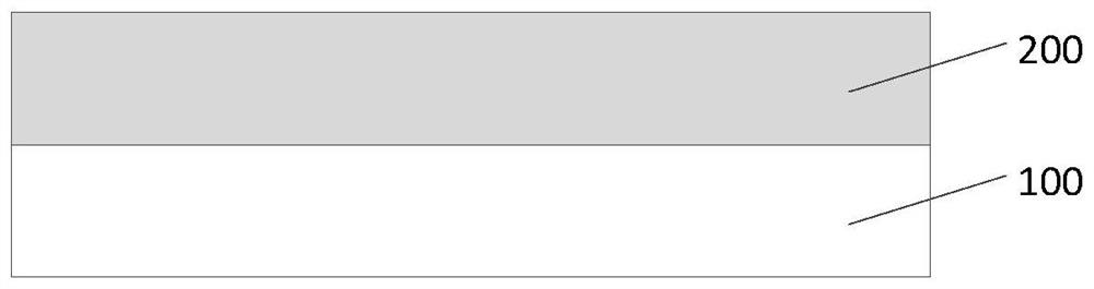
[0044] In order to make the above-mentioned purpose, features and advantages of the present application more obvious and understandable, the specific implementation manners of the present application will be described in detail below in conjunction with the accompanying drawings.

[0045] In the following description, a lot of specific details are set forth in order to fully understand the application, but the application can also be implemented in other ways different from those described here, and those skilled in the art can do it without violating the content of the application. By analogy, the present application is therefore not limited by the specific embodiments disclosed below.

[0046] Secondly, the present application is described in detail in combination with schematic diagrams. When describing the embodiments of the present application in detail, for the convenience of explanation, the cross-sectional view showing the device structure will not be partially enlarged...


PUM

PropertyMeasurementUnit
Thicknessaaaaaaaaaa

Abstract

The embodiment of the invention provides a semiconductor structure and a manufacturing method thereof. The method comprises: providing a silicon substrate, epitaxially forming a germanium film on thesilicon substrate, and epitaxially growing a gallium arsenide film on the germanium film, so that the germanium film is used as a buffer layer between the silicon substrate and the gallium arsenide film layer, improve lattice mismatch between the silicon substrate and the gallium arsenide film layer, reduce a reverse domain in the gallium arsenide film layer, reduce defects in the gallium arsenidefilm layer and improve the performance of a device based on the gallium arsenide film layer.

Description

technical field [0001] The present application relates to the field of semiconductor devices and manufacturing thereof, and in particular to a semiconductor structure and a manufacturing method thereof. Background technique [0002] With the diversification of semiconductor devices, it is necessary to combine a variety of semiconductor materials to form semiconductor devices. In some scenarios, it is necessary to use gallium arsenide (GaAs) materials to prepare detectors, lasers, etc. However, the lattice mismatch between silicon and gallium arsenide is serious, so the epitaxially grown gallium arsenide film layer on the silicon substrate has many defects, and the antiphase domin (APD) is serious. Photoelectric devices based on such gallium arsenide film layer have large dark current and high noise, and it is difficult to obtain a large-area gallium arsenide film layer on a silicon substrate that meets the requirements. Contents of the invention [0003] In view of this, ...

Claims


Application Information

Patent Timeline
IPC IPC(8): H01L21/02H01L29/267
CPCH01L21/02381H01L21/0245H01L21/02546H01L29/267
Inventor 亨利·H·阿达姆松王桂磊杜勇徐步青黎奔
Owner GUANGDONG GREATER BAY AREA INST OF INTEGRATED CIRCUIT & SYST
Why Eureka
Try Eureka