Hot electron effect characterization method based on compound material MISFET device

A hot electron and compound technology, applied in the field of microelectronics reliability characterization, can solve the problems such as the inability to inject hot electrons into the insulating layer, the uneven distribution of hot electrons, and the lack of research and characterization of the mechanism.

Active Publication Date: 2020-09-15
XIDIAN UNIV
View PDF6 Cites 0 Cited by
  • Summary
  • Abstract
  • Description
  • Claims
  • Application Information

AI Technical Summary

Problems solved by technology

[0004] However, when hot electron stress is applied to n-channel MISFET devices with conventional structures, due to the potential difference from the drain to the source, the distribution of hot electrons in the channel is not uniform, and the number of carriers in the channel and its acceleration The electric field strength is simultaneously related to the applied gate-source voltage and gate-drain voltage bias
Therefore, when the thermal electron stress is only applied to the conventional n-channel MISFET device, it is impossible to inject hot electrons uniformly into the insulating layer, and it is also impossible to independently study the influence of the number of hot electron injections and the injection energy on the performance degradation of the device. The mechanism of the electronic effect lacks in-depth research and characterization

Method used


Image

  • Hot electron effect characterization method based on compound material MISFET device
  • Hot electron effect characterization method based on compound material MISFET device
  • Hot electron effect characterization method based on compound material MISFET device

Examples


Embodiment 1

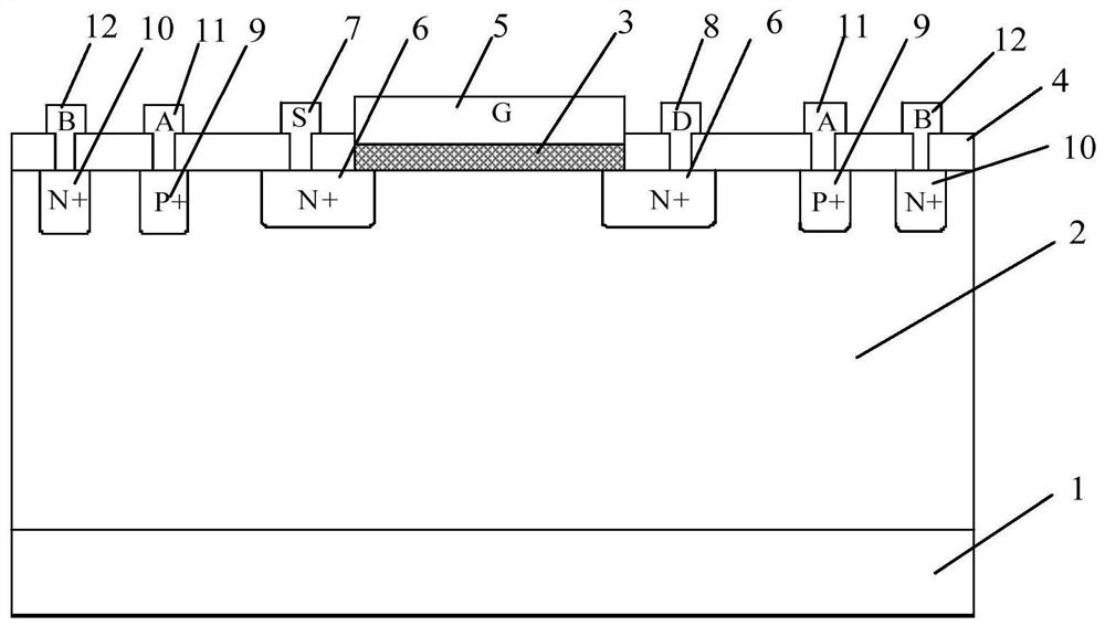
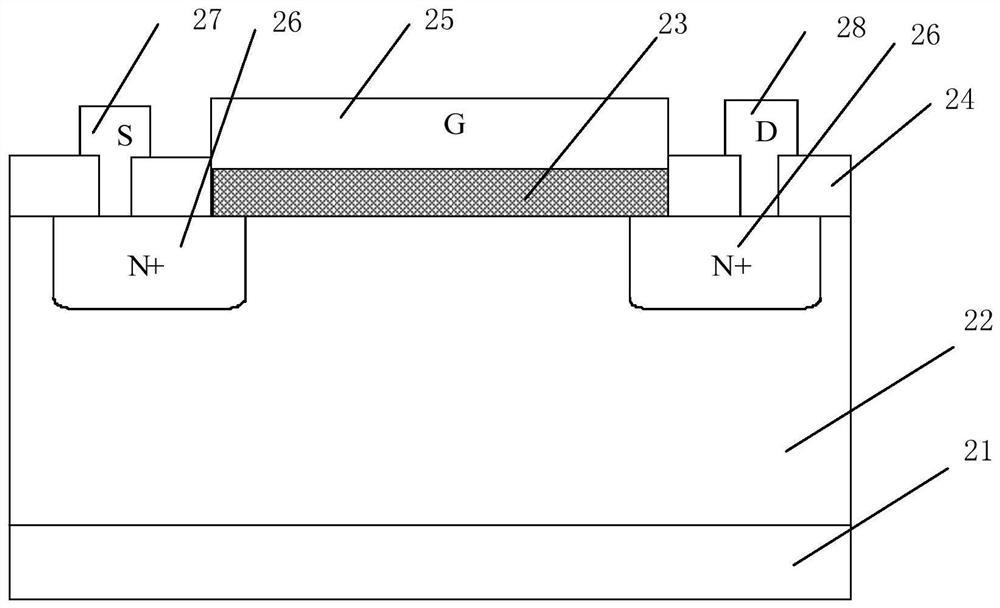
[0057] See figure 1 and figure 2 , figure 1 A structural schematic diagram of a thermal electron effect test structure based on a compound material MISFET device provided by the present invention; figure 2 It is a schematic structural diagram of a compound material-based MISFET device provided by the present invention. This embodiment takes a MISFET device based on compound materials as an example, such as figure 1 shown. A thermal electron effect test structure based on a compound material MISFET device, comprising: a substrate 1, a P-type epitaxial layer 2, an insulating layer 3, a passivation layer 4, a gate 5, a first N+ doped region 6, and a source 7 , drain 8, P+ doped region 9, second N+ doped region 10, electrode A11 and electrode B12; wherein,

[0058] The P-type epitaxial layer 2 is located on the substrate 1;

[0059] The insulating layer 3 is located on the P-type epitaxial layer 2;

[0060] The gate 5 is located on the insulating layer 3;

[0061] The tw...

Embodiment 2

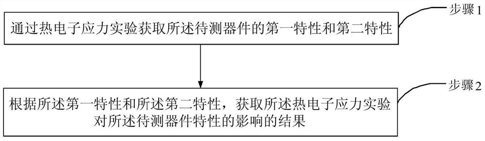
[0072] Please continue to see figure 1 , and see image 3 and Figure 4 . image 3 A schematic flow chart of a thermal electron effect characterization method based on a compound material MISFET device provided by the present invention; Figure 4 It is a schematic circuit connection schematic diagram of a thermal electron effect characterization method based on a compound material MISFET device provided by the present invention. On the basis of the above-mentioned embodiments, this embodiment focuses on the detailed description of the thermal electron effect characterization method based on compound material MISFET devices, such as image 3 shown. Specifically, the following steps are included:

[0073] Obtaining the first characteristic and the second characteristic of the device under test through a thermal electron stress experiment;

[0074] According to the first characteristic and the second characteristic, obtain the result of the influence of the thermal electron...

Embodiment 3

[0097] Please continue to see figure 1 , figure 2 , image 3 and Figure 4 , and see Figure 5 , Figure 6 a-6b and Figure 7 a-7b, Figure 8 a-8b, Figure 5 A flow chart for the realization of a thermal electron effect characterization method based on a compound material MISFET device provided by the present invention; Figure 6 Provide the present invention with a graph showing the degradation of the output characteristics and transfer characteristics of the device under test as they vary with the number of hot electron injections; Figure 7 Provide the present invention with a graph showing the variation of the output characteristics and transfer characteristics of the device under test with different hot electron injection energies; Figure 8 The present invention provides graphs of the degradation of the output characteristics and transfer characteristics of the device under test as they vary with different gate voltages. This embodiment describes the characteri...


PUM


Abstract

The invention relates to a test structure based on a thermo-electronic effect of an MISFET device. The test structure comprises a substrate (1), a P type epitaxial layer (2), an insulating layer (3),a passivation layer (4), a grid electrode (5), a first N+ doped region (6), a source electrode (7), a drain electrode (8), a P+ doped region (9), a second N+ doped region (10), an electrode A (11) andan electrode B (12). The embodiment of the invention provides a heterojunction device test structure of a hot electron injection quantity and energy controllable technology, and a hot electron effectcharacterization method, wherein the injection quantity of hot electrons in a insulating layer is controlled by adjusting a voltage Va and a voltage Vb, and the injection energy of the hot electronsin the insulating layer is controlled by adjusting the voltage Va, so that the problems of uncontrollable hot electron injection quantity and injection energy of the device, non-uniform injection of the insulating layer and the like are solved, and the deep analysis of the hot electron effect in the heterojunction device is facilitated.

Description

technical field [0001] The invention belongs to the technical field of microelectronic reliability characterization, and in particular relates to a thermal electron effect characterization method based on a compound material MISFET device. Background technique [0002] From the first-generation semiconductor materials represented by silicon materials to the second-generation semiconductor materials represented by gallium arsenide materials, to the third-generation semiconductor materials represented by gallium nitride, the material properties have become more and more excellent. High-performance semiconductor devices and even integrated circuits provide a solid material foundation. In particular, the third-generation wide-bandgap semiconductor materials have excellent characteristics such as high breakdown field strength, high thermal conductivity, and high electron saturation drift speed. Semiconductor devices based on them can operate at high power, high frequency, high vo...

Claims


Application Information

Patent Timeline
Patent Type & Authority Applications(China)
IPC IPC(8): H01L23/544G01R31/26
CPCG01R31/2601G01R31/2642H01L22/34
Inventor 郑雪峰李纲王小虎陈管君马晓华郝跃
Owner XIDIAN UNIV
Why Eureka
Try Eureka