Structure for testing hot hole effect of compound MISFET device, and characterization method thereof
A technology for testing structures and hot holes, applied in semiconductor/solid-state device testing/measurement, electrical components, circuits, etc. Hole and other issues
- Summary
- Abstract
- Description
- Claims
- Application Information
AI Technical Summary
Problems solved by technology
Method used
Image
Examples
Embodiment 1
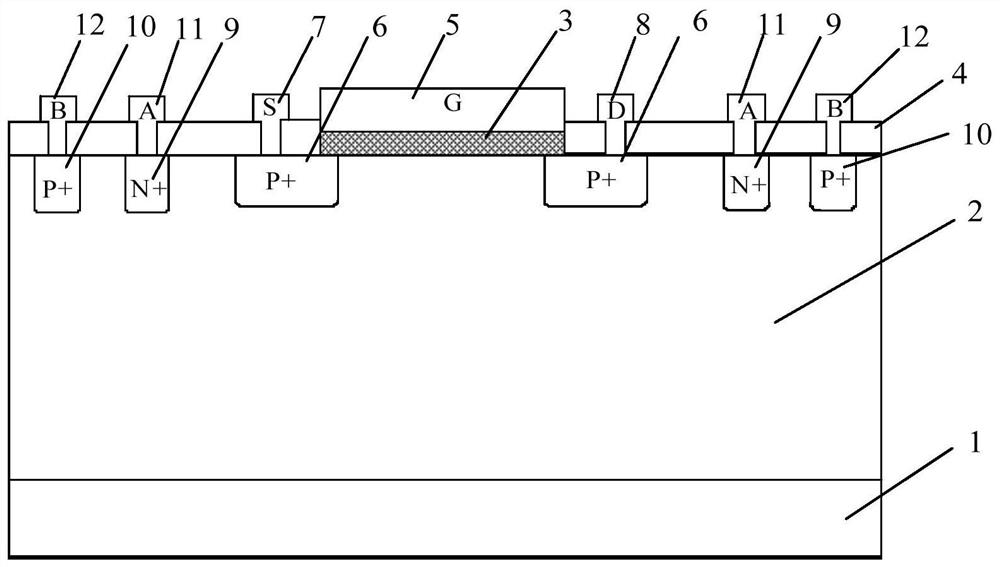
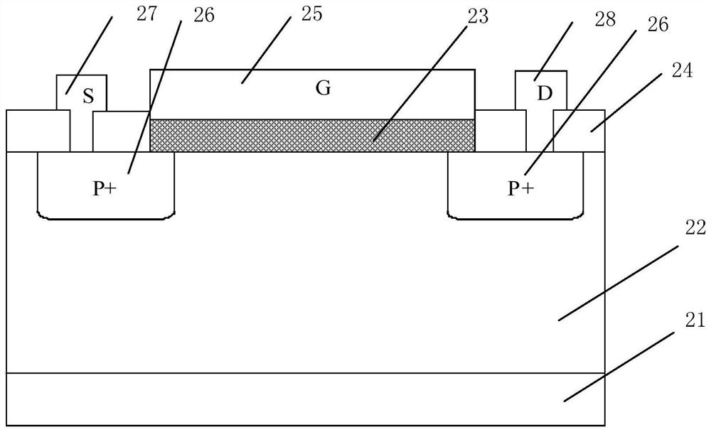
[0057] See figure 1 and figure 2 , figure 1 A schematic diagram of the test structure for the hot hole effect of a compound MISFET device provided by the present invention; figure 2 It is a schematic structural diagram of a compound MISFET device provided by the present invention. This embodiment takes a compound MISFET device as an example, such as figure 1 shown. A test structure for the hot hole effect of a compound MISFET device, comprising: a substrate 1, an N-type epitaxial layer 2, an insulating layer 3, a passivation layer 4, a gate 5, a first P+ doped region 6, a source 7, Drain 8, N+ doped region 9, second P+ doped region 10, electrode A11 and electrode B12; wherein,
[0058] The N-type epitaxial layer 2 is located on the substrate 1;
[0059] The insulating layer 3 is located on the N-type epitaxial layer 2;
[0060] The gate 5 is located on the insulating layer 3;
[0061] The two first P+ doped regions 6 are correspondingly distributed in the N-type epit...
Embodiment 2
[0072] Please continue to see figure 1 , and see image 3 and Figure 4 . image 3 A schematic flow chart of the characterization method for the hot hole effect of a compound MISFET device provided by the present invention; Figure 4 It is a schematic circuit connection schematic diagram of a method for characterization of the hot hole effect of a compound MISFET device provided by the present invention. On the basis of the above-mentioned embodiments, this embodiment focuses on the detailed description of the hot hole effect characterization method based on the compound MISFET device, such as image 3 shown. Specifically, the following steps are included:
[0073] Obtaining the first characteristic and the second characteristic of the device under test through a hot hole stress experiment;
[0074] According to the first characteristic and the second characteristic, obtain the result of the influence of the hot hole stress experiment on the characteristics of the device...
Embodiment 3
[0098] Please continue to see figure 1 , figure 2 , image 3 and Figure 4 , and see Figure 5 , Figure 6 a-6b and Figure 7 a-7b, Figure 8 a-8b, Figure 5 A flowchart for realizing the characterization method of the hot hole effect of a MISFET device provided by the present invention; Figure 6 Provide the present invention with a graph of the degradation of the output characteristics and transfer characteristics of the device under test with different hot hole injection quantities; Figure 7 Provide the present invention with curves of the degradation of the output characteristics and transfer characteristics of the device under test with different hot hole injection energies; Figure 8 The present invention provides graphs of the degradation of the output characteristics and transfer characteristics of the device under test as they vary with different gate voltages. This embodiment describes the characterization method in detail on the basis of the above embodim...
PUM
 Abstract
Description
Claims
Application Information
 - R&D Engineer
- R&D Manager
- IP Professional
- Industry Leading Data Capabilities
- Powerful AI technology
- Patent DNA Extraction
Browse by: Latest US Patents, China's latest patents, Technical Efficacy Thesaurus, Application Domain, Technology Topic, Popular Technical Reports.
© 2024 PatSnap. All rights reserved.Legal|Privacy policy|Modern Slavery Act Transparency Statement|Sitemap|About US| Contact US: help@patsnap.com


