High-sensitivity light receiving device

A light-receiving device and high-sensitivity technology, applied in the field of optical communication, can solve the problems of reducing the optical interface density of switches, low product qualification rate, increasing product cost, etc., to facilitate photoelectric conversion and external output, improve coupling efficiency, and qualify products. high rate effect

Inactive Publication Date: 2020-09-04
湖北协长通讯科技有限公司
View PDF6 Cites 7 Cited by
  • Summary
  • Abstract
  • Description
  • Claims
  • Application Information

AI Technical Summary

Problems solved by technology

However, since the avalanche diode APD belongs to avalanche amplification, it is sensitive to static electricity, and even a small amount of static electricity will cause the chip to be broken down and damaged.
Therefore, on the one hand, the pass rate of the product is low and the product cost is increased; on the other hand, the APD needs a high-voltage power supply (typical value 30V) to produce an electronic avalanche effect and achieve the effect of low signal amplification. The special boost circuit controls the ADP, which leads to an increase in the complexity of the electronic control and a corresponding increase in cost
In addition, the light-receiving device in the prior art occupies a large space, and the miniaturization of the module cannot be carried out.
For example, the current 100G hybrid 40km transmission distance module can only use the CFP2 package, which is nearly 6 times larger than the mainstream 100G QSFP28 package, which significantly reduces the optical interface density on the switch

Method used


Image

  • High-sensitivity light receiving device
  • High-sensitivity light receiving device
  • High-sensitivity light receiving device

Examples


Embodiment Construction

[0031] The principles and features of the present invention are described below in conjunction with the accompanying drawings, and the examples given are only used to explain the present invention, and are not intended to limit the scope of the present invention.

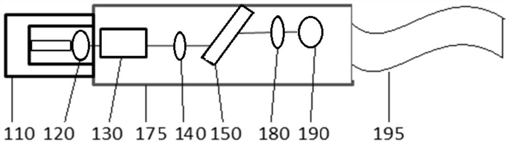
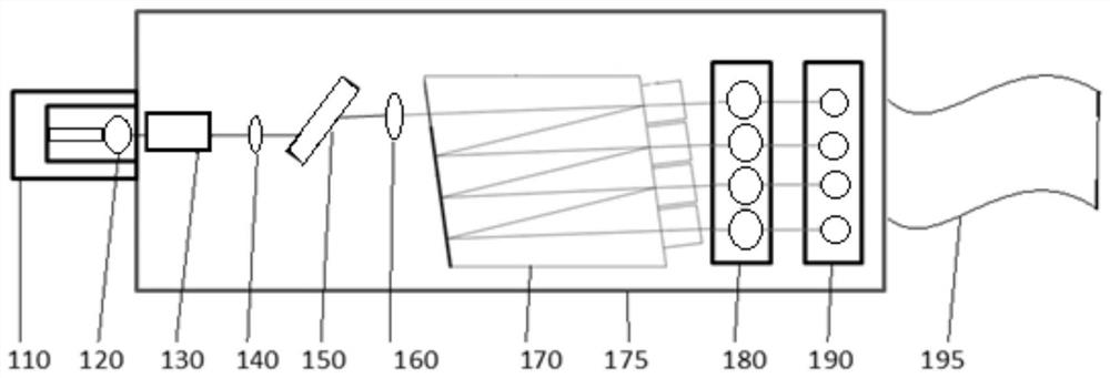
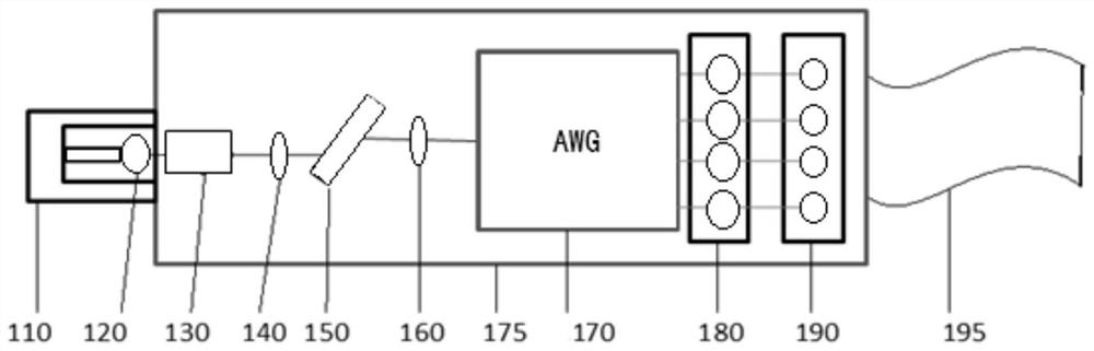
[0032] Such as figure 1 As shown, a single-channel high-sensitivity light-receiving device includes an optical fiber adapter 110, an isolator 130, a casing 175, a first lens 140, a semiconductor optical amplifier 150, a second lens 180, a light detection PIN PD chip 190 and an output The circuit board 195, one end surface of the tube shell 175 is respectively provided with a through hole or a light window for optical signals to pass through, and the optical fiber adapter 110 is arranged on the end of the tube shell 175 with the through hole, so The isolator 130, the first lens 140, the semiconductor optical amplifier 150, the second lens 180 and the photodetection PIN PD chip 190 are packaged in the shell 175 respec...


PUM


Abstract

The invention relates to a high-sensitivity light receiving device. The high-sensitivity light receiving device comprises an optical fiber adapter, an isolator, a tube shell, a first lens, a semiconductor optical amplifier, a second lens, an optical detection PIN PD chip and an output circuit board, wherein through holes are formed in the end surface of one end of the tube shell; the optical fiberadapter is arranged at one end, provided with the through holes, of the tube shell; the isolator, the first lens, the semiconductor optical amplifier, the second lens and the optical detection PIN PDchip are separately packaged in the tube shell and are in optical path connection in sequence; the output end of the optical detection PIN PD chip is electrically connected with one end of the outputcircuit board; and the other end of the output circuit board is electrically connected with an external electric signal receiving device. According to the high-sensitivity optical receiving device, high-sensitivity receiving can be realized, the product percent of pass is high, electric control is simple, and cost is effectively reduced; the semiconductor optical amplifier and the optical detection PIN PD chip are integrated, so that the miniaturization of the device is realized, and the realization of miniaturized single-channel SFP packaging or multi-channel QSFP packaging is facilitated.

Description

technical field [0001] The invention relates to the technical field of optical communication, in particular to a high-sensitivity light receiving device. Background technique [0002] With the explosive growth of Internet data services and the continuous emergence of applications such as cloud computing, high-performance computers, data centers, and autonomous driving, optical fiber communication has higher and higher requirements for communication bandwidth and longer and longer access transmission distances. From tens of meters in the data center to 2km, 10Km, or even 30-40Km. [0003] In the prior art, the solution to the long-distance transmission on the access side is to use an avalanche diode (APD) as a signal detection device to construct a high-sensitivity optical receiving device to achieve the receiving sensitivity required for a transmission distance of 30-40km. However, since the avalanche diode APD belongs to avalanche amplification, it is sensitive to static e...

Claims


Application Information

Patent Timeline
Patent Type & Authority Applications(China)
IPC IPC(8): H04B10/67H04B10/69G02B6/42
CPCG02B6/4204G02B6/4281H04B10/67H04B10/691
Inventor 田志平周火焱施汉林
Owner 湖北协长通讯科技有限公司
Why Eureka
Try Eureka