
Wafer superposition anomaly compensation method and wafer superposition anomaly information measurement method

A compensation method and abnormal information technology, which is applied in semiconductor/solid-state device testing/measurement, microlithography exposure equipment, instruments, etc., can solve the problem of difficult compensation of crystal edge superposition ability, product yield decline, and impact on product yield, etc. problem, to achieve the effect of superposition compensation and improve product yield

Pending Publication Date: 2020-08-25
SHANGHAI HUALI INTEGRATED CIRCUTE MFG CO LTD
View PDF5 Cites 0 Cited by
  • Summary
  • Abstract
  • Description
  • Claims
  • Application Information

AI Technical Summary

Problems solved by technology

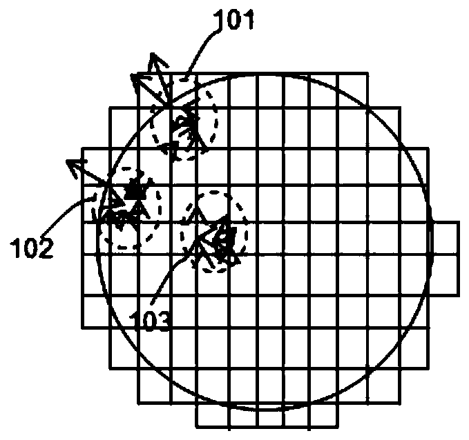
Also, see figure 2 , figure 2 Schematic diagram of anomalous vectors for wafer stacking, such as figure 2 As shown, the superimposed abnormal vector in the exposure unit 103 close to the center of the wafer is relatively small, while the superimposed abnormal vector around the wafer is relatively large, specifically, such as the exposure unit (shot) 101 located at the edge of the wafer and the superposition anomaly vector in the exposure unit 102 is relatively large, and it is easy to exceed the superposition anomaly threshold, resulting in a decline in product yield
And it is very difficult to compensate for the superposition ability of the crystal edge, so it seriously affects the product yield

Method used


Image

  • Wafer superposition anomaly compensation method and wafer superposition anomaly information measurement method
  • Wafer superposition anomaly compensation method and wafer superposition anomaly information measurement method
  • Wafer superposition anomaly compensation method and wafer superposition anomaly information measurement method

Examples


Embodiment Construction

[0026] The technical solutions in the present invention will be clearly and completely described below in conjunction with the accompanying drawings. Apparently, the described embodiments are part of the embodiments of the present invention, not all of them. Based on the embodiments of the present invention, all other embodiments obtained by persons of ordinary skill in the art without making creative efforts belong to the protection scope of the present invention.

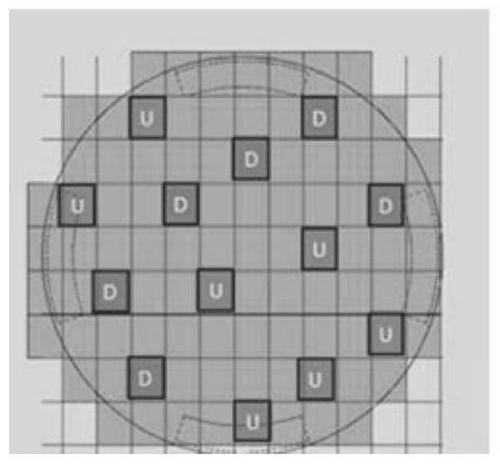
[0027] At present, all superposition abnormality compensation methods are to measure the superposition information in 13 exposure units (shots) on the wafer surface, measure 9 points in each exposure unit, and then measure according to the measured 13 exposures Complement the superposition exception information in the unit. Specifically, see image 3 , image 3 It is a schematic diagram of measurement of abnormal information superimposed on wafers in the prior art, such as image 3 , exposure unit D and exposur...


PUM


Abstract

The invention relates to a wafer superposition anomaly compensation method and relates to the semiconductor integrated circuit fabrication technology. Exposure units used for superposing abnormal measurement are arranged, wherein the number of the exposure units used for superposition anomaly measurement is any value between 25 and 35; the ratio of the number of the exposure units located in the wafer edge range in the exposure units used for superposition anomaly measurement to the number of the exposure units except the wafer edge range in a wafer surface is any value between 4:1 and 6:1; ameasurement point in each exposure unit for superposing abnormal measurement; according to the invention, the number of the measurement points in each exposure unit for superposition anomaly measurement is set to ensure that the numbers of the exposure units located in the exposure units for the superposing abnormal measurement are equal, the information amount proportion of the superposition anomaly in the wafer edge range is increased, so that the obtained wafer superposition anomaly information can better reflect the superposition anomaly information of the wafer edge, the wafer edge superposition compensation effect is better, and the product yield is further improved.

Description

technical field [0001] The invention relates to the manufacturing technology of semiconductor integrated circuits, in particular to a wafer superposition abnormality compensation method. Background technique [0002] In the manufacturing process of semiconductor integrated circuits, superposition abnormalities are often detected in the photolithography area, which leads to a decrease in product yield. In addition, most of the superposition abnormalities appear in the circle around the wafer, that is, the wafer edge, and no matter in the process or on the exposure machine, many of them will cause superposition abnormalities around the wafer edge. Specifically, see figure 1 , figure 1 Overlay exception diagram for PDF wafer, such as figure 1 As shown, most of the superposition anomalies appear in the circle around the wafer. Also, see figure 2 , figure 2 Schematic diagram of superimposed exception vectors for wafers, such as figure 2 As shown, the superimposed abnorm...

Claims


Application Information

Patent Timeline
Patent Type & Authority Applications(China)
IPC IPC(8): G03F7/20H01L21/66
CPCG03F7/7065G03F7/70483H01L22/24
Inventor 刘隽瀚周文湛胡展源
Owner SHANGHAI HUALI INTEGRATED CIRCUTE MFG CO LTD
Learn More